Programmable low noise amplifier and method

a low-noise amplifier and programmable technology, applied in amplifier combinations, amplifier control details, gain control, etc., can solve the problems of high noise, circuit oscillation, and “overload” of strong input signals, and achieve accurate tail current tracking (i)

Active Publication Date: 2006-12-19
TEXAS INSTR INC
View PDF7 Cites 19 Cited by
  • Summary
  • Abstract
  • Description
  • Claims
  • Application Information

AI Technical Summary

Benefits of technology

[0014]It is an object of the present invention to provide a low noise, programmable gain MOS amplifier.
[0015]It is another object of the invention to provide a low noise, programmable gain MOS or CMOS amplifier that can extend the dynamic range of input signals that can be amplified with low distortion.
[0016]It is another object of invention to provide a low noise, programmable gain MOS or CMOS amplifier that is electronically programmable with a single control signal, thereby eliminating parasitic impedances from affecting the amplifier gain.
[0017]It is another object of the invention to provide a low noise, programmable gain CMOS or MOS amplifier which avoids the need for and costs associated with use of an external gain control resistor and the associated amount of area required on a printed circuit board.
[0018]It is another object of invention to provide a low noise, low-cost programmable gain amplifier which achieves both low current noise and low voltage noise.
[0024]In the some described embodiments, the first transistors and second transistors are P-channel transistors, and the switch transistors also are P-channel transistors. The tail current transistor (Q3) is a P-channel transistor having a gate coupled to a gate and drain of a current mirror control transistor (Q2) having a source coupled to the first reference voltage (VDD). A bias control circuit includes an operational amplifier (12) having a first input coupled to a third reference voltage (Vref), an output coupled to a gate of a control transistor (Q1) having a drain coupled to the gate and a drain of the current mirror control transistor (Q2) and a source coupled to a second input of the operational amplifier (12) and a first terminal of a control resistor (14) having a second terminal coupled to the second control voltage (GROUND). The control resistor (14) is composed of the same resistive material as the first (30) and second (32) load resistors, so that accurate tracking of the tail current (I) with respect to temperature and process variations is achieved. A gain select circuit (35) operates in response to a gain select input (36) to produce the desired gain selection signals on the gates of the plurality of switch transistors, respectively.

Problems solved by technology

By way of background, resistance in series between the source electrodes of a pair of differentially coupled MOSFETs is the main source of noise in a differential amplifier.
These parasitic impedances often cause the gain to be imprecise and can lead to circuit oscillation.
The high gain setting is desirable to achieve the lowest noise but will result in “overload” from strong input signals.
Allowing the gain to be reduced results in higher noise, but the amplifier can handle a larger amplitude input signal.
Unfortunately, any resistance connected between the sources of input transistors Q2 and Q3 introduces noise, and therefore the prior programmable gain amplifiers of this kind inherently have relatively high noise compared to the noise of the basic prior art low noise amplifier 1 of FIG. 1.
The prior techniques of using external switches to selectively switch external resistors so as to control the gain of an amplifier is costly and inconvenient because of the physical size, and also reduces circuit performance because of parasitic capacitances associated with the external resistor and switch.

Method used


Image

  • Programmable low noise amplifier and method
  • Programmable low noise amplifier and method
  • Programmable low noise amplifier and method

Examples


Embodiment Construction

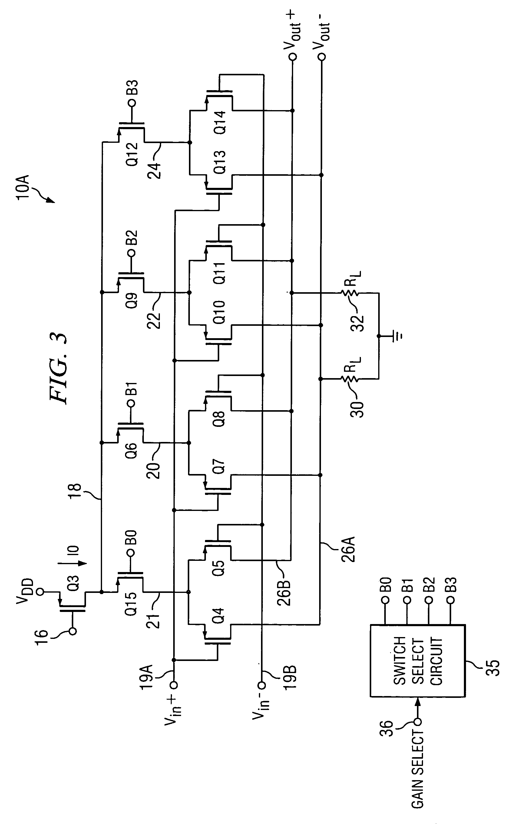
[0029]Referring to FIG. 2, low noise programmable differential amplifier 10 includes a bias circuit including an operational amplifier 12 having its (+) input coupled to a reference voltage Vref, its output connected to the gate of a N-channel transistor Q1, and its (−) input connected to the source of transistor Q1. A resistor 14 having a resistance RB is connected between ground and the source of transistor Q1. The drain of transistor Q1 is connected by conductor 16 to the drain of a P-channel current mirror control transistor Q2 and to the gates of transistor Q2 and a P-channel current mirror output transistor Q3, referred to herein as tail current transistor Q3. A tail current I0 flows through tail current transistor Q3 by virtue of the operation of the above mentioned bias circuit and transistor Q2 to achieve tracking of tail current I0 width respect to temperature and processing parameters associated with control resistor 14 and subsequently mentioned load resistors 30 and 32....


PUM


Abstract

A programmable gain low noise amplifier includes a tail current transistor (Q3) having a source coupled to a first reference voltage (VDD) and a drain coupled to a tail current conductor (18) and, in a differential input embodiment, a plurality of pairs (Q4,5, Q7,8, Q10,11, Q13,14) of differentially coupled input transistors. Each pair includes a first input transistor having a gate coupled to a first input conductor (19A) and a drain coupled to a first output conductor (26A) and a second input transistor having a gate coupled to a second input conductor (19B), a source coupled to a source of the first transistor, and a drain coupled to a second output conductor (26B). The sources of the first and second input transistors of some or all of the pairs are selectively coupled to the tail current conductor (18) in it response to corresponding gain control signals (B1,2,3).

Description

BACKGROUND OF THE INVENTION[0001]The present invention relates generally to low noise amplifiers, and more particularly to low noise amplifiers having programmable gain.[0002]By way of background, resistance in series between the source electrodes of a pair of differentially coupled MOSFETs is the main source of noise in a differential amplifier. The prior art circuit shown in FIG. 1 illustrates a very low noise differential amplifier 1 which includes a P-channel current source transistor Q1 having its drain connected directly by a conductor 2 to the sources of a pair of P-channel input transistors Q2 and Q3. The drains of input transistors Q2 and Q3 are connected by output conductors 3 and 4 to load resistors 5, and 6, which have a resistance RL. Input voltages Vin+ and Vin− are applied to the gates of input transistors Q2 and Q3, respectively, and output voltages Vout− and Vout+ are produced on output conductors 3 and 4, respectively. The reason that the noise of amplifier 1 is ve...

Claims


Application Information

Patent Timeline
Patent Type & Authority Patents(United States)
IPC IPC(8): H03F3/45
CPCH03F3/45183H03F3/68H03G1/0023H03G1/0029H03G1/0088H03F2200/372H03F1/26H03F3/45
Inventor KOEN, MYRON J.VENKATARAMAN, HARISH
Owner TEXAS INSTR INC
Why Eureka
Try Eureka