
Radiation shielding of integrated circuits and multi-chip modules in ceramic and metal packages

a technology of integrated circuits and multi-chip modules, which is applied in the direction of radiation controlled devices, semiconductor devices, semiconductor/solid-state device details, etc., can solve the problems of inability to adequately shield the semiconductor device from the hazards encountered in spacecraft environment, unreliable device operation, and semiconductor device to malfunction in a relatively short tim

Inactive Publication Date: 2006-12-12
MAXWELL TECH INC
View PDF13 Cites 37 Cited by
  • Summary
  • Abstract
  • Description
  • Claims
  • Application Information

AI Technical Summary

Benefits of technology

The solution effectively reduces radiation exposure to silicon integrated circuit dies, ensuring reliable operation in harsh spacecraft environments while minimizing weight and manufacturing costs, providing nearly 4π coverage for radiation protection.

Problems solved by technology

Unfortunately, these devices are susceptible to electromagnetic interference which can cause the operation of the device to be unreliable.
While the shielding of the semiconductor devices described in these Japanese patent publications are capable of preventing malfunctions due to EMI, they cannot adequately shield the semiconductor device from the hazards encountered in a spacecraft environment.
The spacecraft environment hazards, including high energy electron, proton, and cosmic ray damage, penetrate the relatively thin protective layer afforded by the EMI shielding, causing the semiconductor device to malfunction in a relatively short time.
As discussed previously, EMI shielding is not adequate to protect the semiconductor device from the hazards encountered in the spacecraft environment.
Typical silicon integrated circuit plastic packaged devices fail to operate when exposed to total doses of two to fifteen kilorads.
The design and manufacture of such a radiation tolerant die is both expensive and difficult, thus many commercially available integrated circuit and multi-chip modules are not available for radiation tolerant applications.
As a result, commercially available packaged silicon integrated circuit devices for use in a spacecraft environment such as low earth orbit, geostationary, or deep space probe, are not feasible.
Although the protective box is effective in shielding its contents from harmful X-rays, this approach has the serious disadvantage of adding substantial bulk and weight to electronic circuit assemblies protected in this manner.
Moreover, it would be expensive to provide this type of protection to individual integrated circuits as manufacturing custom boxes for each circuit configuration would undoubtedly be costly.
While the projections aid in protecting the semiconductor from harmful radiation, they also add weight.
The additional weight is critical and very undesirable in space applications.
Although such a double layered shield film arrangement could be capable of providing some protection for a semiconductor device from radiation, the shielding is not acceptable for some applications.
Under such an incredible force, the upper shield film is subject to tearing off from the sealing cover.
Furthermore, the use of a double layer shield film only slightly reduces the weight of the package.
It also increases the size of the package unnecessarily.
The amount of shielding required to protect the semiconductor unnecessarily increases the weight and expense of such a semiconductor device.
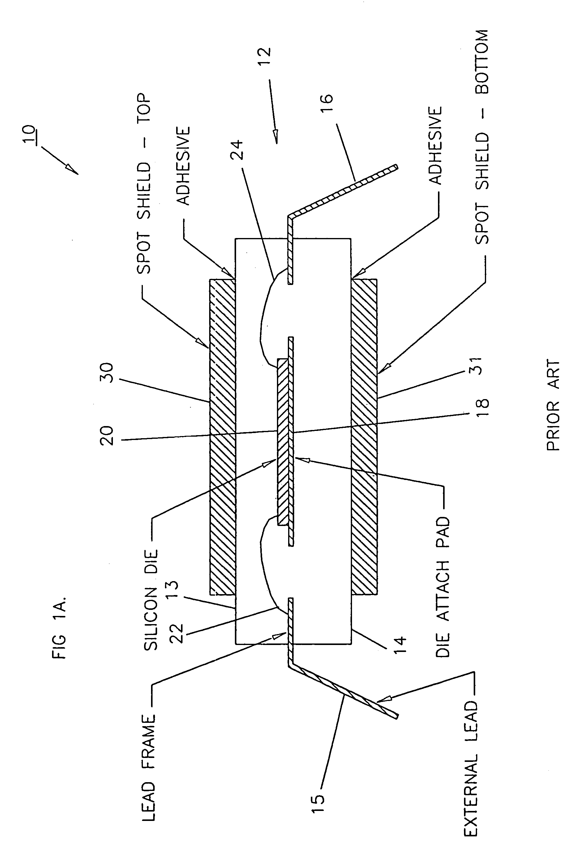
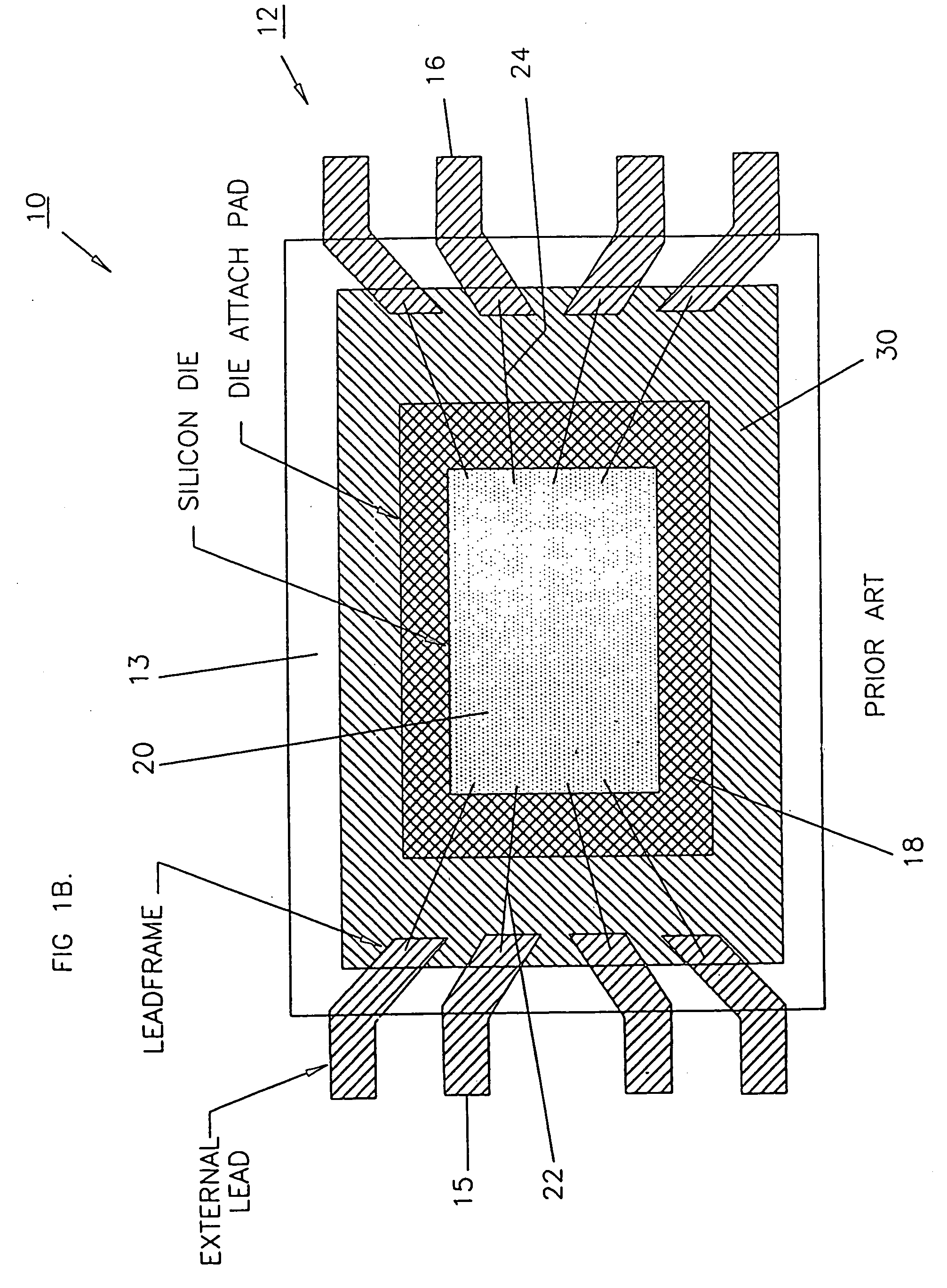
Significant disadvantages of the spot shielding method include an increase in the thickness of the device, increased weight of the device, and increased exposure of the semiconductor to side angle radiation due to the shielding being spaced apart from the semiconductor.
In addition, a bottom spot shield often cannot be used due to the offset in height which cannot be accommodated by a fixed device lead length.
This causes problems when the bottom shield is used on a semiconductor device in conjunction with a printed circuit board in a through hole package style.
Furthermore, the spot shielded packaged semiconductor integrated circuit device provides no mechanical support for the spot shields except for the adhesive used to attach it to the surface of the package.

Method used


Image

  • Radiation shielding of integrated circuits and multi-chip modules in ceramic and metal packages
  • Radiation shielding of integrated circuits and multi-chip modules in ceramic and metal packages
  • Radiation shielding of integrated circuits and multi-chip modules in ceramic and metal packages

Examples


example 1

[0135]Tungsten 90% by weight

[0136]Copper 10% by weight

example 2

[0137]Tungsten 80% by weight

[0138]Copper 20% by weight

example 3

[0139]Tungsten 85% by weight

[0140]Copper 15% by weight

[0141]To fabricate the shield members, sheets of the high and low Z materials can be laminated together in the proper proportions. Alternatively, the shield members may be fabricated by admixing the preferred proportions of powdered high Z and low Z substances together. The high Z and low Z substances are then compressed and stamped. The heat generated by this process leads to heat binding of the radiation shield member components.

[0142]Any high Z material may be used with any low Z material, and one or more, including three or more such materials can be combined. Three or even four different substances, or more, may be combined to satisfy the preferred composition for the shield member.


PUM


Abstract

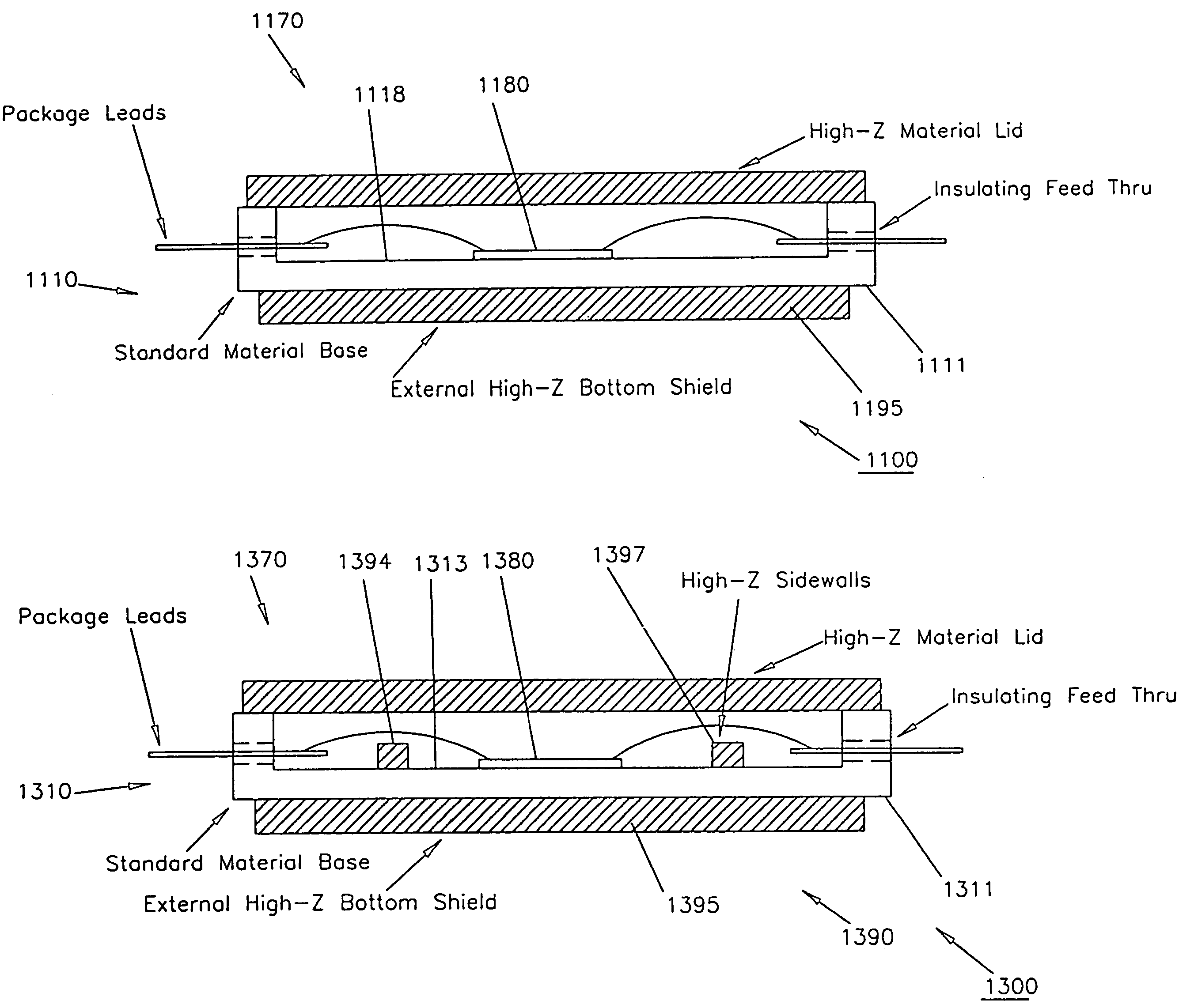
A radiation shielded and packaged integrated circuit semiconductor device includes a lid secured to a base to enclose an integrated circuit die within, wherein the lid and the base are each constructed from a high Z material to prevent radiation from penetrating therethrough. Another embodiment includes a die attach slug constructed from a high Z material disposed between the integrated circuit die and the base, in combination with a high Z material lid to substantially block incident radiation.

Description

CROSS-REFERENCE TO RELATED PATENT APPLICATIONS[0001]This application is a Division of U.S. application Ser. No. 09 / 456,631, filed Dec. 8, 1999 now U.S. Pat. No. 6,720,493, currently pending, which is a Continuation-in-part of U.S. application Ser. No. 09 / 375,881, filed Aug. 17, 1999, which issued as U.S. Pat. No. 6,261,508 on Jul. 17, 2001, which is a Continuation-in-part of U.S. application Ser. No. 08 / 791,256, filed Jan. 30, 1997, now abandoned, which is a Continuation-in-part of U.S. application Ser. No. 08 / 372,289, filed Jan. 13, 1995, which issued as U.S. Pat. No. 5,635,754 on Jun. 30, 1997, which is a Continuation-in-part of U.S. application Ser. No. 08 / 221,506, filed Apr. 1, 1994 now abandoned. This application claims priority to all the foregoing applications and as such the present application hereby claims a priority date of Apr. 1, 1004. This application hereby incorporates by reference all of the above referenced patents and patent applications as if fully set forth here...

Claims


Application Information

Patent Timeline
Patent Type & Authority Patents(United States)
IPC IPC(8): H01L21/44H01L21/48H01L21/50H01L23/055H01L23/057H01L23/18H01L23/29H01L23/31H01L23/552H01L25/065H05K9/00
CPCH01L23/055H01L23/057H01L23/18H01L23/295H01L23/3135H01L23/552H01L25/0655H01L2224/48091H01L2224/48137H01L2224/4823H01L2224/48247H01L2224/49171H01L2924/01078H01L2924/01079H01L2924/14H01L2924/15153H01L2924/15165H01L2924/15312H01L2924/15787H01L2924/16152H01L2924/1616H01L2924/1617H01L2924/16195H01L2924/167H01L2924/3025H01L2924/00014H01L24/48H01L24/49H01L2924/01322H01L2924/00H01L2924/10253H01L2224/32225H01L2224/05599H01L2224/45099H01L2224/85399H01L2924/181H01L2224/05553H01L2924/10161H01L2224/45015H01L2924/207H01L2924/00012
Inventor STROBEL, DAVID J.CZAJKOWSKI, DAVID R.
Owner MAXWELL TECH INC
Learn More