
Complete-charge-transfer vertical color filter detector

a detector and color filter technology, applied in the field of digital image capture, can solve the problems of not being practical for three-color applications, difficult and expensive to manufacture devices, and unable to meet the needs of three-color applications,

Inactive Publication Date: 2006-11-07
FOVEON
View PDF35 Cites 93 Cited by
  • Summary
  • Abstract
  • Description
  • Claims
  • Application Information

AI Technical Summary

Problems solved by technology

These devices are difficult and expensive to manufacture and have not been practical for three-color applications.
Examples of this technology are disclosed in U.S. Pat. No. 4,677,289 entitled “Color Sensor” and U.S. Pat. No. 4,651,001 titled “Visible / Infrared Imaging Device with Stacked Cell Structure.” These structures are also difficult and expensive to produce and have not become practical.
Such sensors have the disadvantage of occupying a relatively large area per pixel as these sensors are tiled together in a plane.
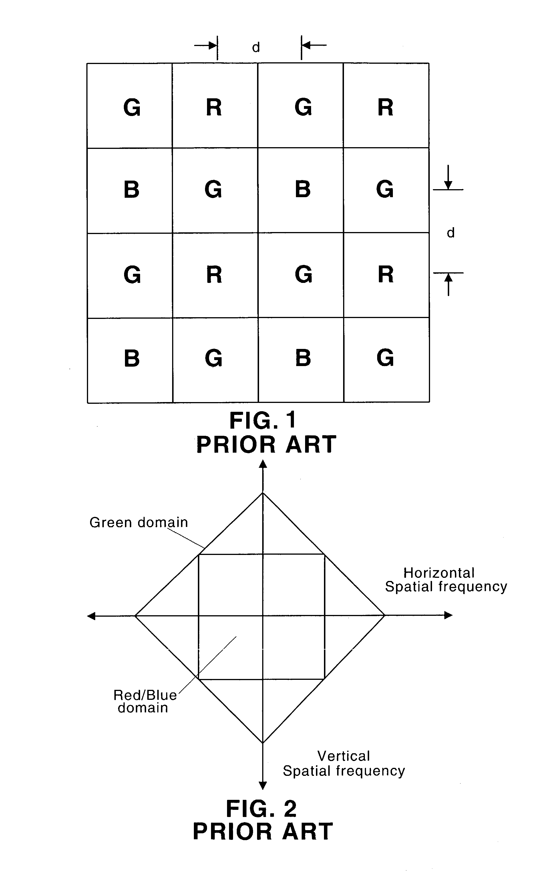
Mosaic approaches are well known in the art to be associated with aliasing problems due to the sensors being small compared to the spacing between sensors so that the sensors locally sample the image signal, and that the sensors for different colors are in different locations, so that the samples may not align between colors.
The device disclosed in the Carr patent has several shortcomings, the most notable being its large area, rendering it unsuitable for the image sensor density requirements of modern imaging systems.
The technology employed for contact formation to the buried infrared sensing diode is also not suitable for modern imaging technology or extension to a three-color sensor.

Method used


Image

  • Complete-charge-transfer vertical color filter detector
  • Complete-charge-transfer vertical color filter detector
  • Complete-charge-transfer vertical color filter detector

Examples


Embodiment Construction

[0038]Persons of ordinary skill in the art will realize that the following description of the present invention is only illustrative and not in any way limiting. Other embodiments of this invention will be readily apparent to those skilled in the art having benefit of this disclosure.

[0039]The advantage of a complete-charge-transfer vertical-color-filter detector group is that each pixel location in the array measures three spectral components at the same location, thus minimizing or eliminating the need for interpolation as required by the Bayer patterns. A further advantage of a full RGB imager formed from complete-charge-transfer vertical-color-filter detector groups is that all of the red, green, and blue image information captured for a single pixel location is contained within a smaller space than in the pixel cluster of prior art imaging systems. This smaller space for capture allows finer resolution of the image.

[0040]In a typical system in accordance with this invention, th...


PUM


Abstract

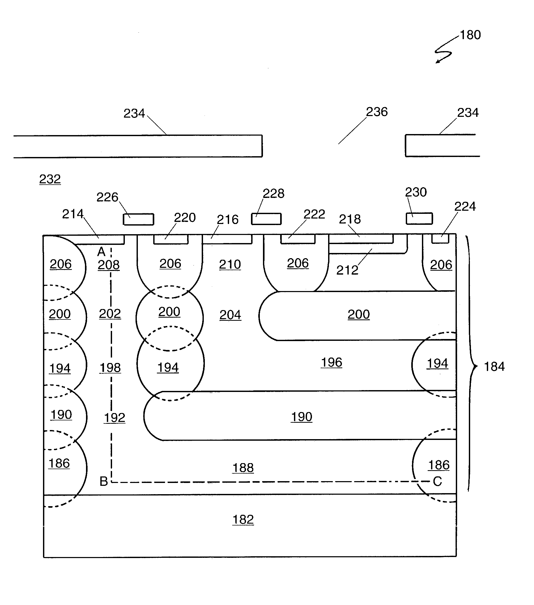
A vertical-color-filter detector disposed in a semiconductor structure comprises a complete-charge-transfer detector comprising semiconductor material doped to a first conductivity type and has a horizontal portion disposed at a first depth in the semiconductor structure substantially below an upper surface thereof and a vertical portion communicating with the upper surface of the semiconductor structure. The complete-charge-transfer detector is disposed within a first charge container forming a potential well around it. The horizontal portion of the complete-charge-transfer detector has a substantially uniform doping density in a substantially horizontal direction and the vertical portion of the complete-charge-transfer detector has a doping density that is a monotonic function of depth and is devoid of potential wells. A first charge-transfer device is disposed substantially at an upper surface of the semiconductor structure and is coupled to the vertical portion of the complete-charge-transfer detector.

Description

RELATED APPLICATIONS[0001]This application is a continuation-in-part of prior co-pending application Ser. No. 09 / 884,863 filed on Jun. 18, 2001 and assigned to the same assignee as the present invention, now U.S. Pat. No. 6,727,521, which claims the benefit of U.S. Provisional Patent Application No. 60 / 235,249, filed on Sep. 25, 2000.BACKGROUND OF THE INVENTION[0002]1. Field of the Invention[0003]The present invention relates to the capture of digital images. More particularly, the present invention relates to complete-charge-transfer vertical-color-filter detectors and arrays thereof.[0004]2. The Prior Art[0005]Semiconductor devices for measuring the color of light are known in the non-imaging art. These devices have been built with a variety of technologies that depend upon the variation of photon absorption depth and wavelength. Examples are disclosed in U.S. Pat. No. 4,011,016 entitled “Semiconductor Radiation Wavelength Detector” and U.S. Pat. No. 4,309,604 entitled “Apparatus ...

Claims


Application Information

Patent Timeline
IPC IPC(8): H01L31/00H01L27/146H01L31/10H04N5/335
CPCH01L27/14621H01L27/14647H01L27/146H01L31/10H04N25/00
Inventor MERRILL, RICHARD B.
Owner FOVEON
Learn More