
Room temperature synthesis of multiwalled carbon nanostructures

a carbon nanostructure and multi-walled technology, applied in the field of room temperature synthesis of multi-walled carbon nanostructures, can solve the problems of substantially increasing the cost of industrial production, producing cnts in high-temperature, etc., and achieve the effect of improving the quality of carbon nanostructures and speeding up reaction speed

Active Publication Date: 2006-11-07
HONG KONG CITY UNIV OF
View PDF0 Cites 8 Cited by
  • Summary
  • Abstract
  • Description
  • Claims
  • Application Information

AI Technical Summary

Benefits of technology

[0008]Preferably the method may be carried out at room temperature and pressure, though the reaction would be speeded up if bath sonication is used. Higher temperatures and pressures, however, would improve the quality of the carbon nanostructures.

Problems solved by technology

This type of process substantially increases the cost of industrial production.
414, 506, 2001) by arc discharge using graphite electrodes in water under room temperature have been reported, one of the challenging issues is to produce CNTs in high-quality (without any metal catalysts) and large quantity within a short time.

Method used


Image

  • Room temperature synthesis of multiwalled carbon nanostructures
  • Room temperature synthesis of multiwalled carbon nanostructures
  • Room temperature synthesis of multiwalled carbon nanostructures

Examples


example 1

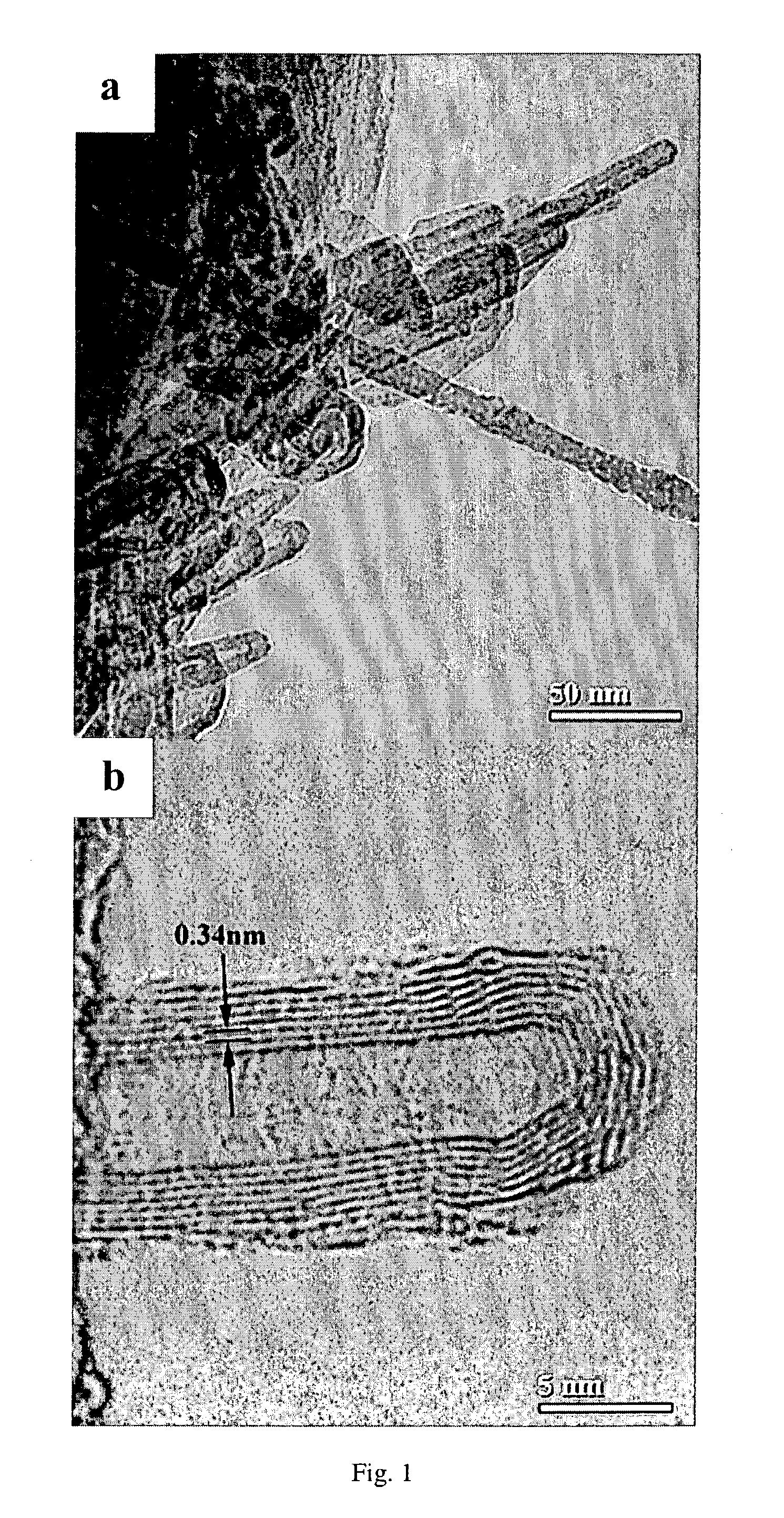
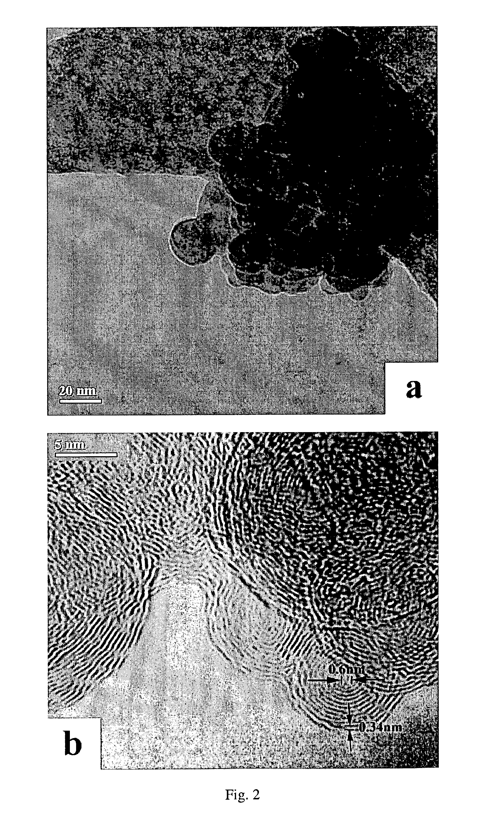
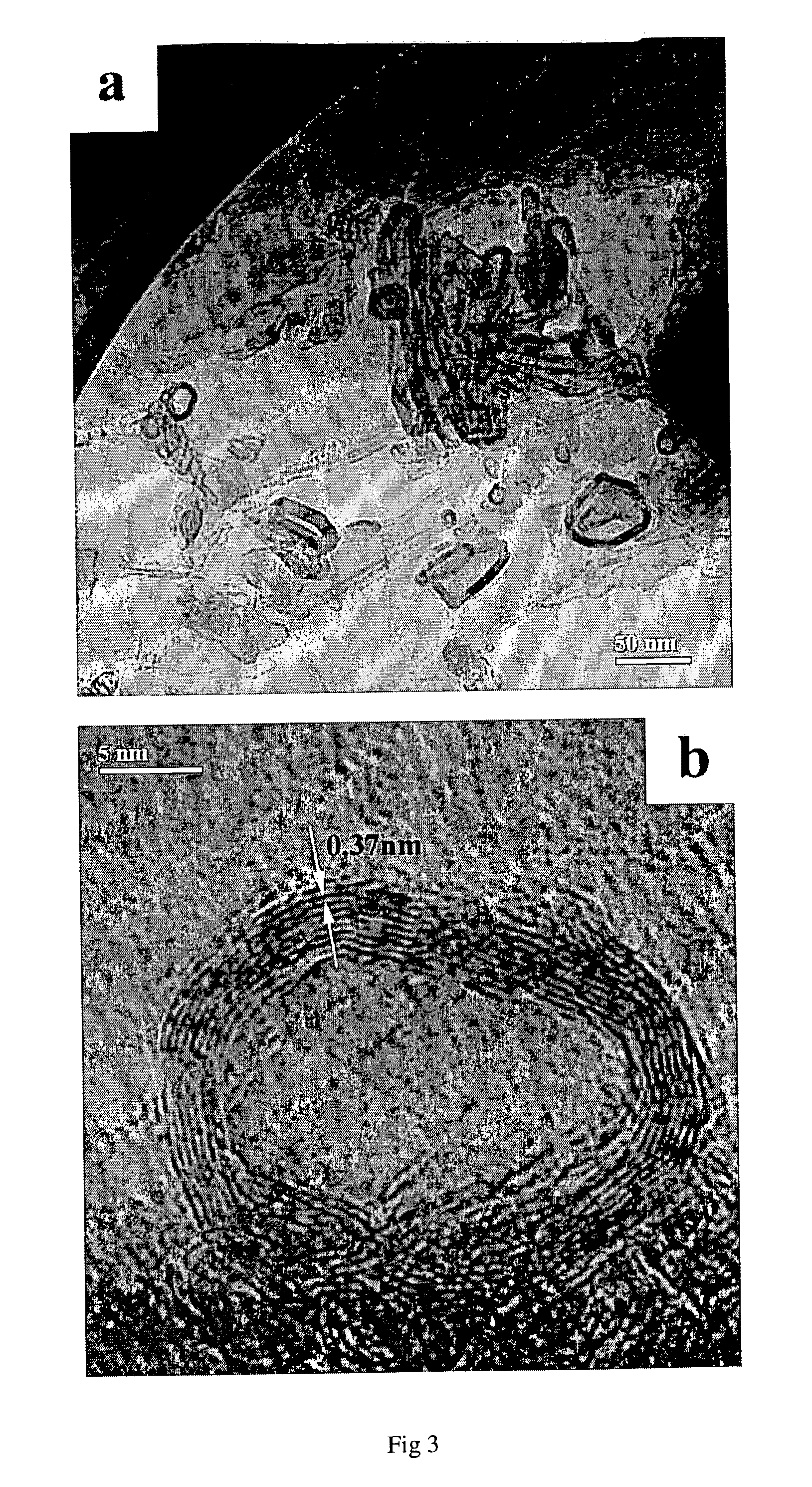
[0023]Silicon nanowires (SiNWs) were used to produce carbon nanostructures. Silicon nanowires, which can be synthesized by thermal evaporation of SiO, are long and freestanding wires with a diameter of several nm to tens of nm, depending upon the preparation conditions and are usually sheathed by a silicon oxide layer. SiNWs were immersed in 5% HF aqueous solution for 5 minutes to remove their oxide outer layer. The HF-etched SiNWs were transferred to a solution of CHCl3 (Lab-Scan 99.5%) immediately and dispersed by bath sonication for 15 minutes at room temperature and atmospheric pressure. The solution changed to colloidal in appearance. High-resolution transmission electron microscopy (HRTEM, Philips CM200 FEG, operated at 200 KeV) samples were prepared by putting a few drops of the resulting solution onto the “holey” carbon grids and dried in air. The morphology and microstructure of products of carbon nanostructures synthesized by this method are shown in FIGS. 1–4 and 6 to 9FI...

example 2

[0031]Silicon nanoparticles were used as the starting material in this example. Silicon nanoparticles were prepared by etching silicon nanoparticle chains in 5% HF aqueous solution for 5 minutes. Silicon nanoparticles were transferred to the solvent of C6H6 (Acros, 99.9%) and sonicated for 15 minutes at room temperature and atmospheric pressure. The solution changed to colloidal in appearance. High-resolution transmission electron microscopy (HRTEM, Philips CM200 FEG, operated at 200 KeV) samples were prepared by putting a few drops of the resulting solution onto the “holey” carbon grids and dried in air. The morphology and microstructure of products of carbon nanostructures synthesized by this method are shown in FIG. 5.

[0032]FIG. 5 shows a HREM image of a Si nanodots covered by 5 layers of carbon sheets with a d-spacing of 4.5 Å.

[0033]It will thus be seen that the present invention, at least in its preferred forms, provides a simple method for forming carbon nanostructures based o...


PUM


Abstract

A simple chemical technique has been developed to grow large quantity of carbon nanostructures, including carbon nanotubes, hydrocarbon nanotubes and carbon nanoonions, in the organic solution at ambient (room) temperature and atmospheric pressure using silicon nanostructures (nanowires, nanodots, ribbons, and porous silicon) as starting materials. These CNT and CNO have the lattice d-spacing from 3.4 Å to 5 Å.

Description

FIELD OF THE INVENTION[0001]The present invention relates to a method of using carbon-containing organic solvents and non-carbon nanostructures (for example silicon nanowires, nanodots and porous silicon) as starting materials for the growth of carbon nanostructures such as multi-walled carbon nanotubes (MWCNT), multi-walled carbon nanoonions (MWCNO) and hydrocarbonate nanotubes (HCNT) in solutions at ambient temperature and pressure.BACKGROUND OF THE INVENTION[0002]Materials engineering at the nanometer scale can provide smaller devices than those currently available. In particular, research on semiconductor nanostructures with size-dependent optical and electronic properties, such as quantum-dots, one-dimensional quantum wire transistors and light emitting devices with extremely low power consumption is motivated by potential applications. Carbon is a material of great interest for nanostructures because of its important role in the field of microelectronics.[0003]Carbon nanotubes...

Claims


Application Information

Patent Timeline
IPC IPC(8): B05D7/00C01B31/02
CPCB82Y30/00B82Y40/00C01B31/0226C01B31/0293C01B2202/06Y10S428/901Y10S428/903C01B32/16C01B32/18
Inventor LEE, SHUIT-TONGLI, CHI-PUISUN, XU-HUIWONG, NING-BEWLEE, CHUN-SINGTEO, BOON-KENG
Owner HONG KONG CITY UNIV OF
Learn More