Balun
a technology of balun and amplitude, applied in the field of balun, can solve the problem of unbalanced signal outputting from the unbalanced terminal, and achieve the effect of small insertion loss and small difference in amplitud
- Summary
- Abstract
- Description
- Claims
- Application Information
AI Technical Summary
Benefits of technology
Problems solved by technology
Method used
Image
Examples
first embodiment
[First Embodiment]
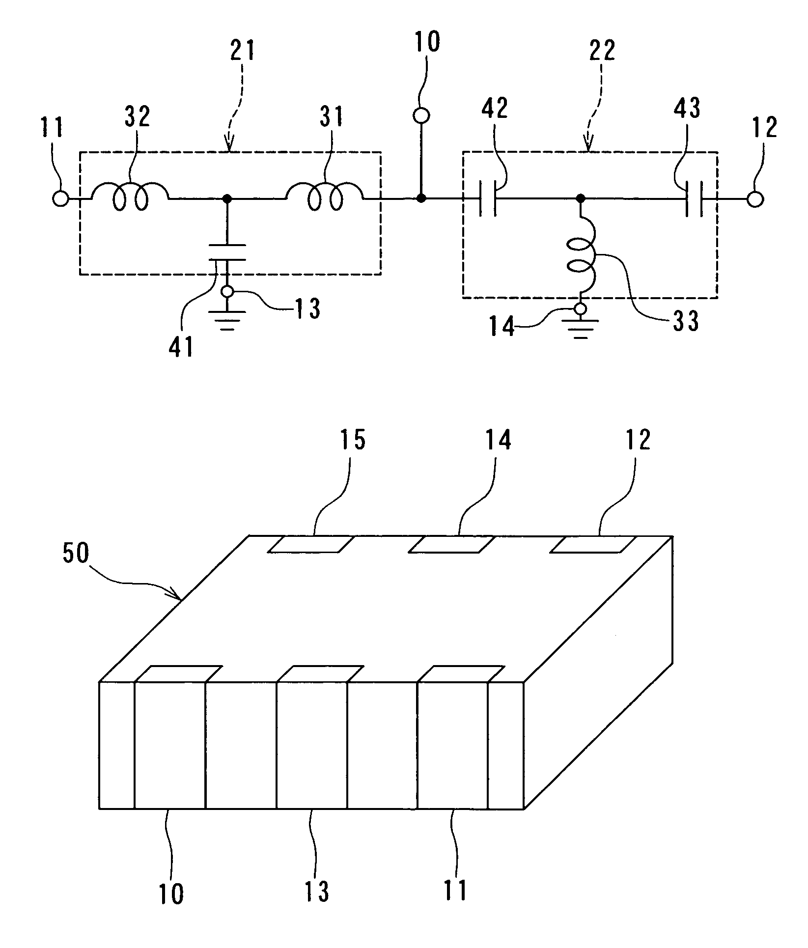
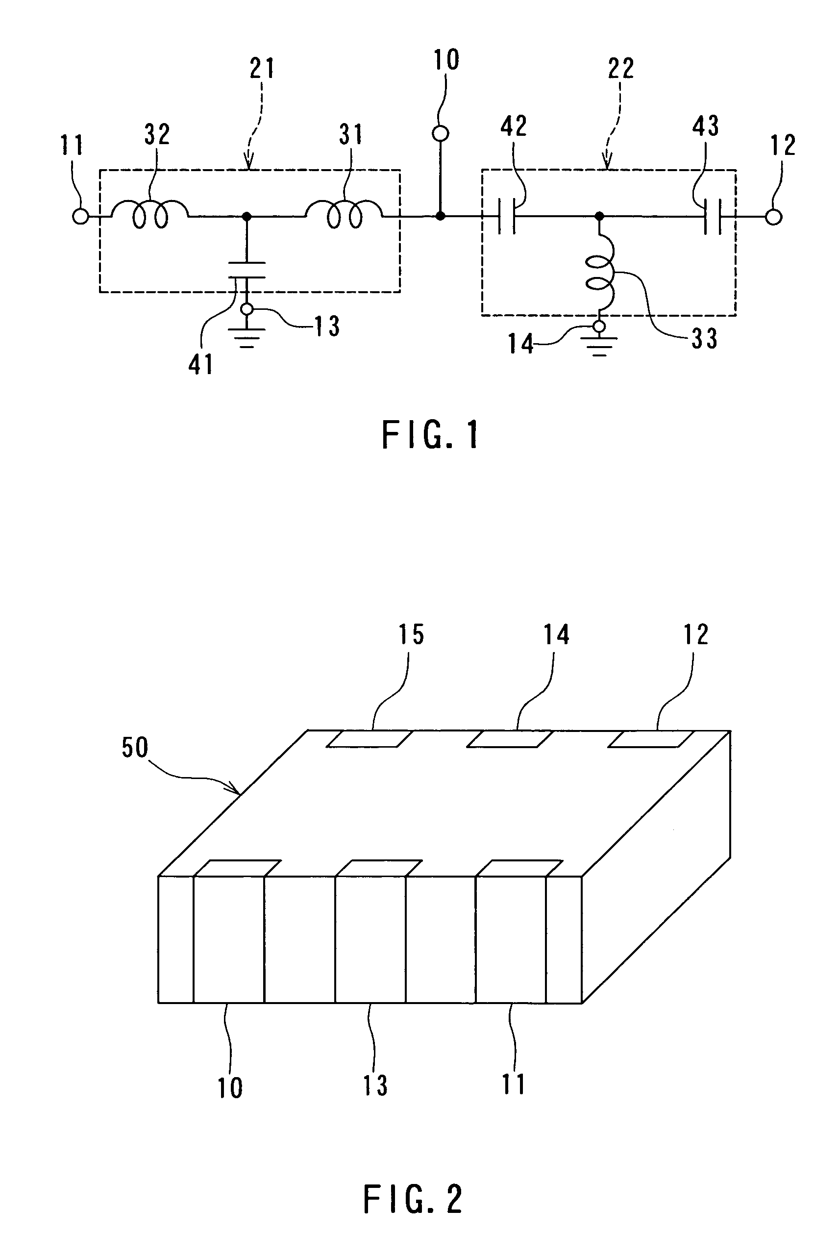
[0049]Reference is now made to FIG. 1 to describe the circuit configuration of a balun of a first embodiment of the invention. The balun of the embodiment comprises: an unbalanced terminal 10 for receiving and outputting unbalanced signals; a first balanced terminal 11 and a second balanced terminal 12 for receiving and outputting balanced signals; and two ground terminals 13 and 14 connected to the ground. The balun further comprises: a low-pass filter 21 provided between the unbalanced terminal 10 and the first balanced terminal 11; and a high-pass filter 22 provided between the unbalanced terminal 10 and the second balanced terminal 12.
[0050]The low-pass filter 21 incorporates: a first coil 31 having an end connected to the unbalanced terminal 10; a second coil 32 having an end connected to the other end of the first coil 31 and having the other end connected to the first balanced terminal 11; and a first capacitor 41 having an end connected to the other end of ...
second embodiment
[Second Embodiment]
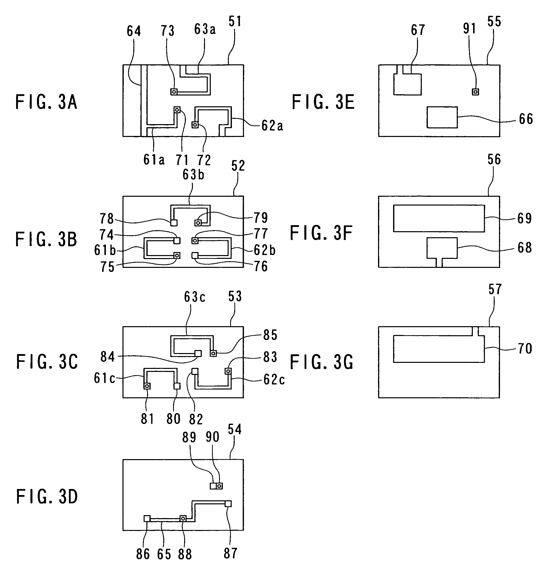
[0083]Reference is now made to FIG. 20A to FIG. 20G to describe a balun of a second embodiment of the invention. FIG. 20A to FIG. 20G illustrate examples of configurations of layers of the multi-layer substrate 50 making up the balun of the second embodiment. FIG. 20A to FIG. 20G illustrate first to seventh conductor layers from the top and a dielectric layer therebelow. In the embodiment the layers of FIG. 20D to FIG. 20G have configurations the same as those of the layers of FIG. 3D to FIG. 3G.
[0084]According to the second embodiment, on the top surface of the dielectric layer 51, as shown in FIG. 20A, a conductor layer 93 for separating coils is formed in addition to the conductor layers of FIG. 3A. The conductor layer 93 is T-shaped and disposed to divide the three regions in which the conductor layers 61a, 62a and 63a for the coils are located. The conductor layer 93 is connected to the ground terminal 13. The dielectric layer 51 has a plurality of through ho...
third embodiment
[Third Embodiment]
[0089]Reference is now made to FIG. 21 to describe a balun of a third embodiment of the invention. FIG. 21 is a schematic diagram illustrating the circuit configuration of the balun of the third embodiment.
[0090]The low-pass filter 21 of the third embodiment incorporates a coil 34 and a capacitor 44 in addition to the coils 31 and 32 and the capacitor 41 of FIG. 1. The coil 34 is inserted between the coil 32 and the first balanced terminal 11. The capacitor 44 has an end connected to the node between the coil 32 and the coil 34. The capacitor 44 has the other end connected to the ground terminal 13.
[0091]The high-pass filter 22 of the third embodiment incorporates a capacitor 45 and a coil 35 in addition to the capacitors 42 and 43 and the coil 33 of FIG. 1. The capacitor 45 is inserted between the capacitor 43 and the second balanced terminal 12. The coil 35 has an end connected to the node between the capacitor 43 and the capacitor 45. The coil 35 has the other e...
PUM
| Property | Measurement | Unit |
|---|---|---|
| capacitance | aaaaa | aaaaa |
| inductance | aaaaa | aaaaa |
| capacitances | aaaaa | aaaaa |
Abstract
Description
Claims
Application Information
 - R&D
- Intellectual Property
- Life Sciences
- Materials
- Tech Scout
- Unparalleled Data Quality
- Higher Quality Content
- 60% Fewer Hallucinations
Browse by: Latest US Patents, China's latest patents, Technical Efficacy Thesaurus, Application Domain, Technology Topic, Popular Technical Reports.
© 2025 PatSnap. All rights reserved.Legal|Privacy policy|Modern Slavery Act Transparency Statement|Sitemap|About US| Contact US: help@patsnap.com


