Frequency-doubling delay locked loop
a delay lock and frequency-doubling technology, applied in the direction of pulse automatic control, static storage, instruments, etc., can solve the problems of analog plls suffering from a number of general drawbacks, pll-based clock generation systems are generally unsuitable, and plls are also unsuitabl
- Summary
- Abstract
- Description
- Claims
- Application Information
AI Technical Summary
Benefits of technology
Problems solved by technology
Method used
Image
Examples
first embodiment
[0026]A frequency-doubling DLL according to the invention is illustrated in FIG. 2(a). An N-stage period-matched DLL (with N being divisible by 4) is used to provide (N−1) outputs TAP[N−1], where each delay stage 20 provides one TAP[i] output. The first N / 2 delay stages outputs are connected to N / 4 2-input tap output generator or “TOG” cells as shown in FIG. 2(a). Dummy loads 25 are coupled on upper N / 2 outputs to keep TPD uniform.
[0027]More specifically, the I (in-phase or 0 degree) and Q (quadrature or 90 degree) inputs to the 2-input TOG cell are connected to delay elements N / 4 stages apart. For example, if N=32, the TOG cell 21 would receive inputs TAP[0] and TAP[8], TOG cell 22 would receive inputs TAP[1] and TAP[9] and so forth up to TOG cell 23 which would receive inputs TAP[7] and TAP[15]. Two outputs, true (T) and complimentary (C), are generated by each TOG cell; for example following the element numbering from above, outputs PHI[0] and PHI[N / 4] for TOG cell 21, outputs PH...
second embodiment
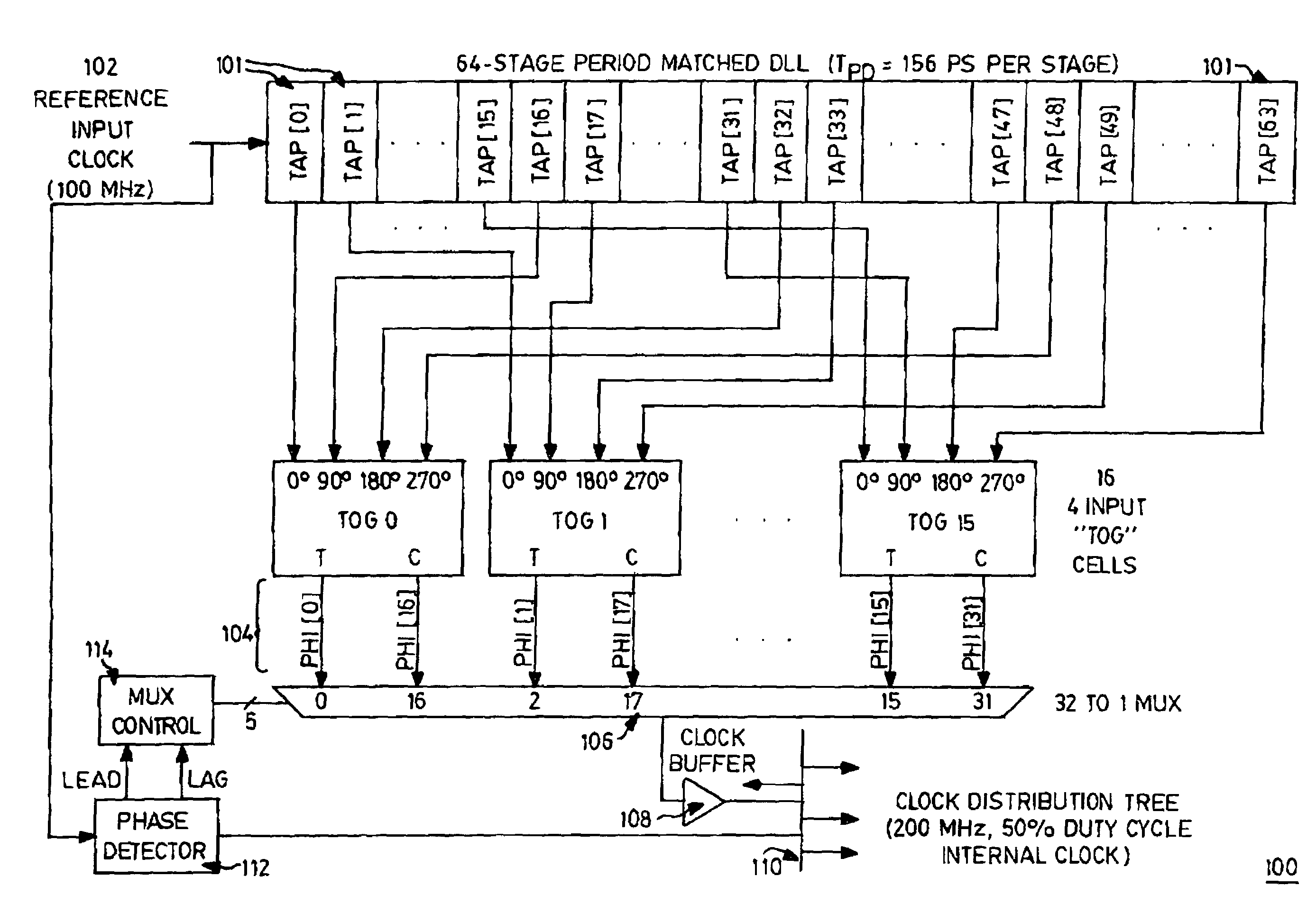
[0039]For applications where the phase relationship between the reference input clock and the frequency doubled internal clock is important, the N / 2 output clock phases from the frequency doubling DLL can be fed to the inputs of a N / 2 to 1 multiplexer. By adding a phase detector and MUX control logic, it is possible to chose the most appropriate clock phase from the N / 2 clock phase outputs. A full clock generating scheme comprising the frequency doubling DLL with duty cycle correction invention for use in a memory interface ASIC is represented generally in FIG. 6 by the numeral 100 having a plurality of serial delay elements 101. In this implementation, N=64 stages and the input reference clock 102 is nominally 100 MHz (Tcp=10.0 ns). It can be seen that the resolution depends on the number of delay elements 101. The DLL generates 32 phases 104 of a 50% duty cycle 200 MHz clock with each phase output spaeed 720 / 64 or 11.25 degrees apart. A 32-input multipleKer 106 selects 1-of-32 pha...
PUM
 Abstract
Description
Claims
Application Information
 - R&D
- Intellectual Property
- Life Sciences
- Materials
- Tech Scout
- Unparalleled Data Quality
- Higher Quality Content
- 60% Fewer Hallucinations
Browse by: Latest US Patents, China's latest patents, Technical Efficacy Thesaurus, Application Domain, Technology Topic, Popular Technical Reports.
© 2025 PatSnap. All rights reserved.Legal|Privacy policy|Modern Slavery Act Transparency Statement|Sitemap|About US| Contact US: help@patsnap.com


