Asymmetric waveguide GaInAs laser diode

a laser diode and waveguide technology, applied in the field of long-wavelength laser diodes, can solve the problems of degrading device performance and reducing slope efficiency, and achieve the effects of reducing operating current, reducing optical loss, and increasing luminous efficiency

Inactive Publication Date: 2006-09-26
SAMSUNG ELECTRONICS CO LTD
View PDF3 Cites 0 Cited by
  • Summary
  • Abstract
  • Description
  • Claims
  • Application Information

AI Technical Summary

Benefits of technology

[0009]The present invention provides a laser diode designed to increase luminous efficiency while lowering operating current by reducing optical loss caused by free carrier absorption in a p-cladding layer.
[0013]This invention changes a symmetric waveguide structure used for a semiconductor laser diode having a waveguide structure, in particular, GaInNAs laser diode into an asymmetric waveguide structure, thus reducing free carrier absorption.

Problems solved by technology

Optical loss due to free carrier absorption in the p-cladding layer increases threshold current of a GaInNAs long-wavelength laser diode while reducing slope efficiency that is a change in output with respect to increase in current, thus degrading the performance of the device.

Method used


Image

  • Asymmetric waveguide GaInAs laser diode
  • Asymmetric waveguide GaInAs laser diode
  • Asymmetric waveguide GaInAs laser diode

Examples


Embodiment Construction

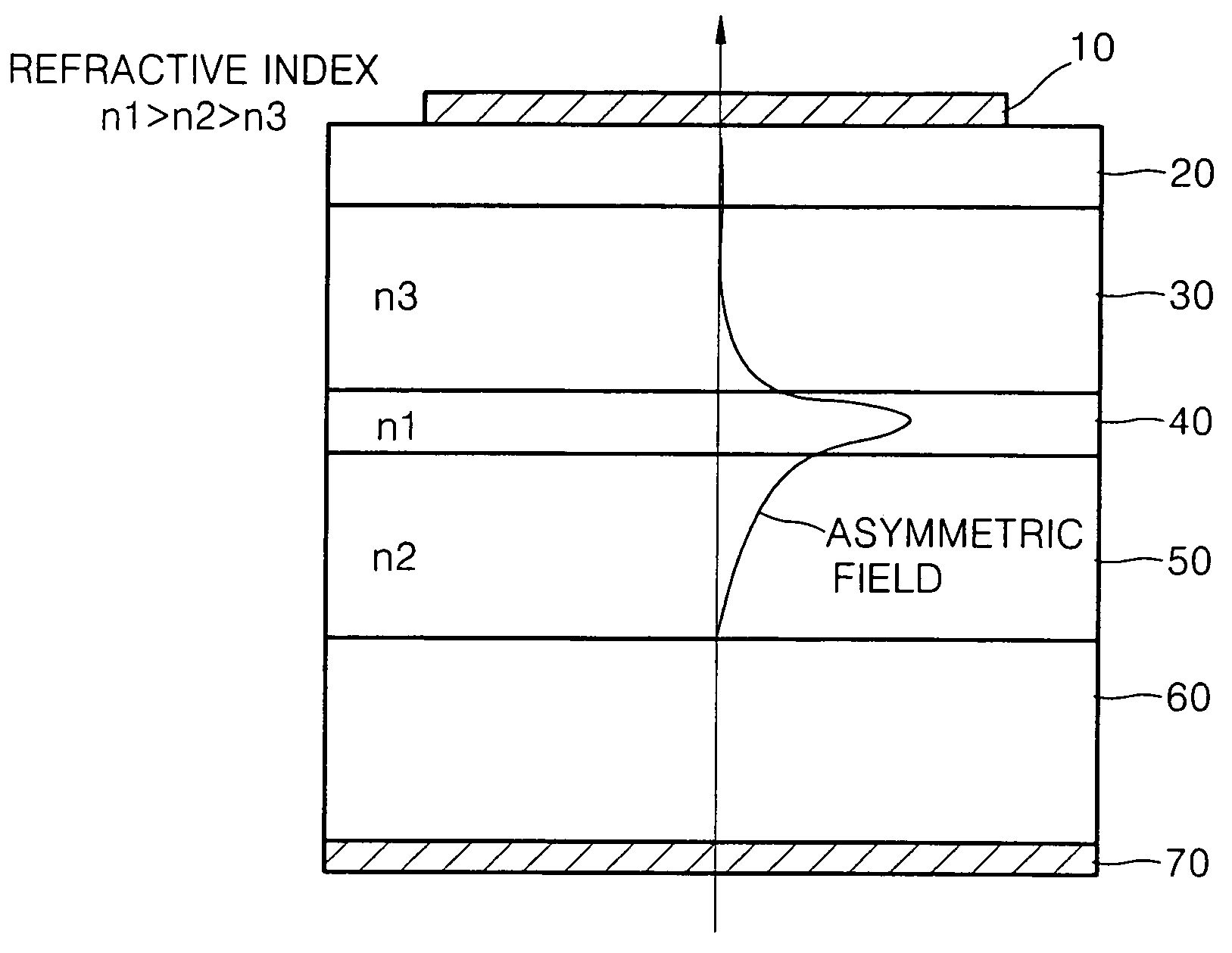
[0021]A laser diode according to an embodiment of this invention will now be described. It should be noted that in the drawings, the thickness and height of each layer constituting a laser diode is exaggerated for clarity.

[0022]Referring to FIG. 4, a semiconductor laser diode includes a GaAs substrate 60, an n-Al0.3Ga0.7As lower cladding layer 50, a Ga1-xInxNyAs1-y (GaInNAs / GaAs or GaInNAs / GaNAs) active layer 40, and a p-Al0.5Ga0.5As upper layer 30. On the upper cladding layer 30, a contact layer 20 and a p-electrode 10 are formed. An n-electrode 70 is formed on the bottom surface of the substrate 6. Here, a first surface of the active layer 40 faces the substrate while a second face thereof faces the opposite direction. Thus, the n-lower cladding layer 50 and the upper n-cladding layer 30 are disposed on the first and second faces of the active layer 40, respectively.

[0023]Here, the active layer 40 may have a single quantum well or multiple quantum well structure. The active layer ...


PUM


Abstract

A laser diode is provided. The laser diode has a structure in which reflective index of an n-cladding layer formed on a first face of the active layer is higher than that of a p-cladding layer formed on a second face. This asymmetric waveguide structure suppresses extension of field into the p-cladding layer thus reducing free carrier absorption in the p-cladding layer.

Description

[0001]This application claims the priority of Korean Patent Application No. 2003-28872, filed on May 7, 2003, the contents of which are incorporated herein by reference in their entirety.BACKGROUND OF THE INVENTION[0002]1. Field of the Invention[0003]The present invention relates to a long-wavelength laser diode, and more particularly, to a GaInNAs laser diode having an asymmetric waveguide structure.[0004]2. Description of the Related Art[0005]U.S. Pat. No. 5,904,549 discloses a GaInAs laser diode. The GaInNAs laser diode, which is a long-wavelength laser device, has a structure as shown in FIG. 1.[0006]Referring to FIG. 1, the conventional GaInAs laser diode is comprised of a GaAs substrate 6, an n-AlxGa1-xAs lower cladding layer 5, a Ga1-xInxNyAs1-y active layer 4, and a p-AlxGa1-xAs upper cladding layer 3. On the upper cladding layer 3, a contact layer 2 and a p-electrode 1 are formed. An n-electrode 7 is formed on the bottom surface of the substrate 6.[0007]The conventional las...

Claims


Application Information

Patent Timeline
Patent Type & Authority Patents(United States)
IPC IPC(8): H01S5/00H01S5/20H01L35/24H01S3/0941H01S5/30H01S5/32H01S5/343
CPCB82Y20/00H01S5/343H01S5/2004H01S5/3213H01S5/305H01S3/0941
Inventor SONG, DAE-SUNGKIM, TAK
Owner SAMSUNG ELECTRONICS CO LTD
Why Eureka
Try Eureka