Power amplifier

a power amplifier and amplifier technology, applied in the direction of amplifiers with dc-coupled stages, amplifiers with semiconductor devices/discharge tubes, amplifier modifications to reduce non-linear distortion, etc., can solve the problem of limiting the modulation swing, the number of non-linear errors and distortion products, and the substantial frequency-independent distortion figure. problem, to achieve the effect of keeping fast reaction speed, and low distortion products in the output signal

Inactive Publication Date: 2006-09-26
KONINKLIJKE PHILIPS ELECTRONICS NV
View PDF10 Cites 23 Cited by
  • Summary
  • Abstract
  • Description
  • Claims
  • Application Information

AI Technical Summary

Benefits of technology

[0005]It is an object of the invention to provide a power amplifier of high quality which has a less complicated structure.
[0006]For this purpose, the power amplifier as described in the opening paragraph, is characterized in that the control circuit is connected between the power output signal and a linear input of the input means for controlling both the gain in the operational frequency range and also said alternately switching of the switching means, said linear input being substantially free of hysteresis. The measures have the advantage that a low output impedance of the amplifier is achieved, even at the filter resonance frequency. Further, a large reduction of inductor-related distortion and a very wide loop bandwidth are achieved, resulting in substantially frequency-independent distortion figures.
[0008]In an embodiment of the power amplifier, the switching means comprises a first switching unit for switching to the first supply voltage and a second switching unit for switching to the second supply voltage, and the input means comprises a voltage comparator having complementary current outputs for respectively driving the first and second switching units. This has the advantage that due to the symmetrical construction of the circuit, distortion products in the output signal are kept low. In an embodiment of the power amplifier, the voltage comparator comprises a difference amplifier and a switching current mirror providing said complementary current outputs. A result of this is that none of the transistors in this circuit are used in saturation, insuring fast reaction speeds.
[0009]In an embodiment of the power amplifier, the switching means comprises a first switching unit for switching to the first supply voltage and a second switching unit for switching to the second supply voltage, both switching units being substantially identical. This has the advantage that due to the symmetrical construction of the circuit, distortion products in the output signal are kept low.

Problems solved by technology

Further, a large reduction of inductor-related distortion and a very wide loop bandwidth are achieved, resulting in substantially frequency-independent distortion figures.
Although such “hysteresis-controlled” oscillating amplifiers may appear relatively uncomplicated, Applicant has seen that such hysteresis results in a number of non-linear errors and distortion products.
Further, the switching frequency may vary with modulation index, limiting the modulation swing.

Method used


Image

  • Power amplifier
  • Power amplifier
  • Power amplifier

Examples


Embodiment Construction

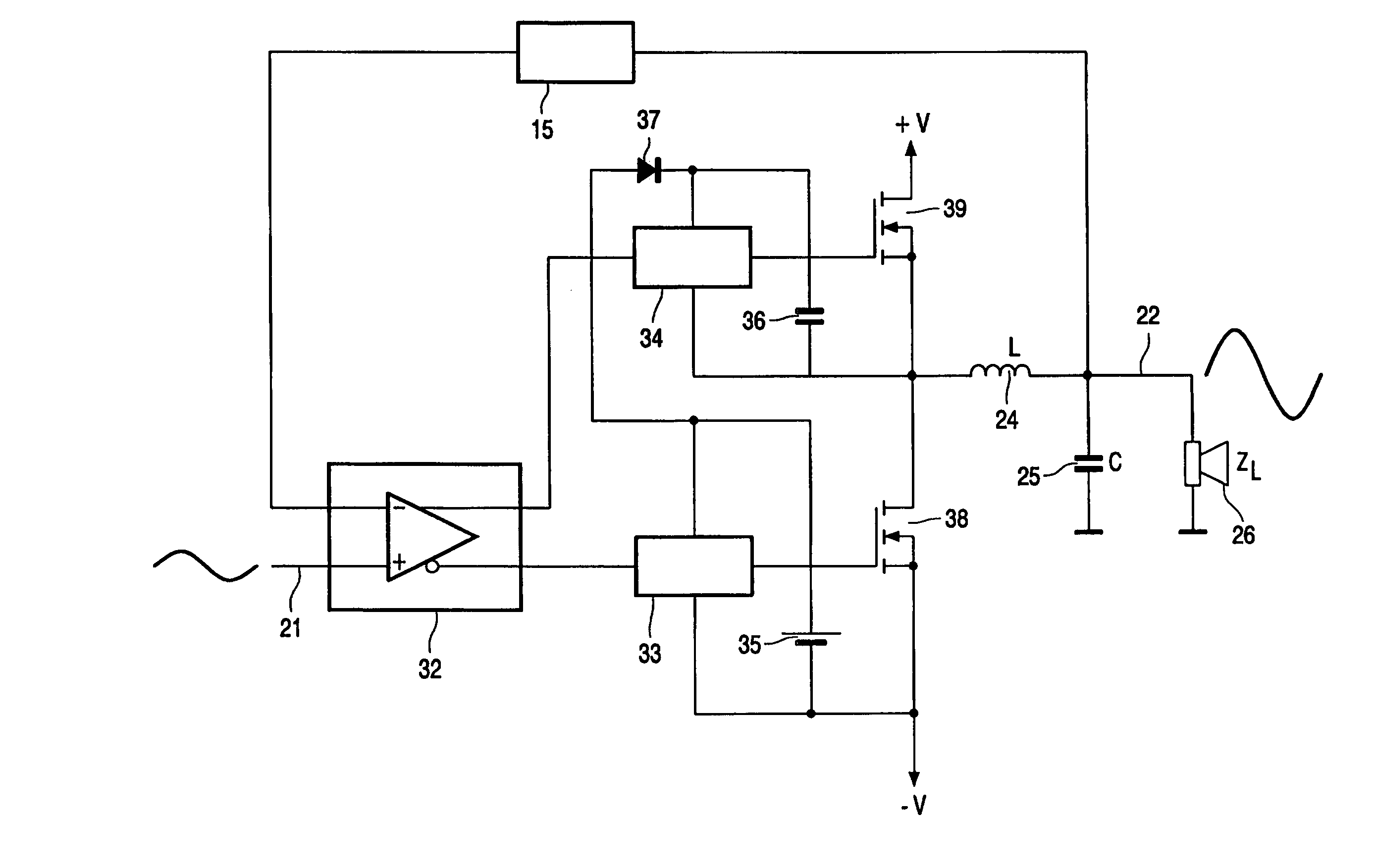
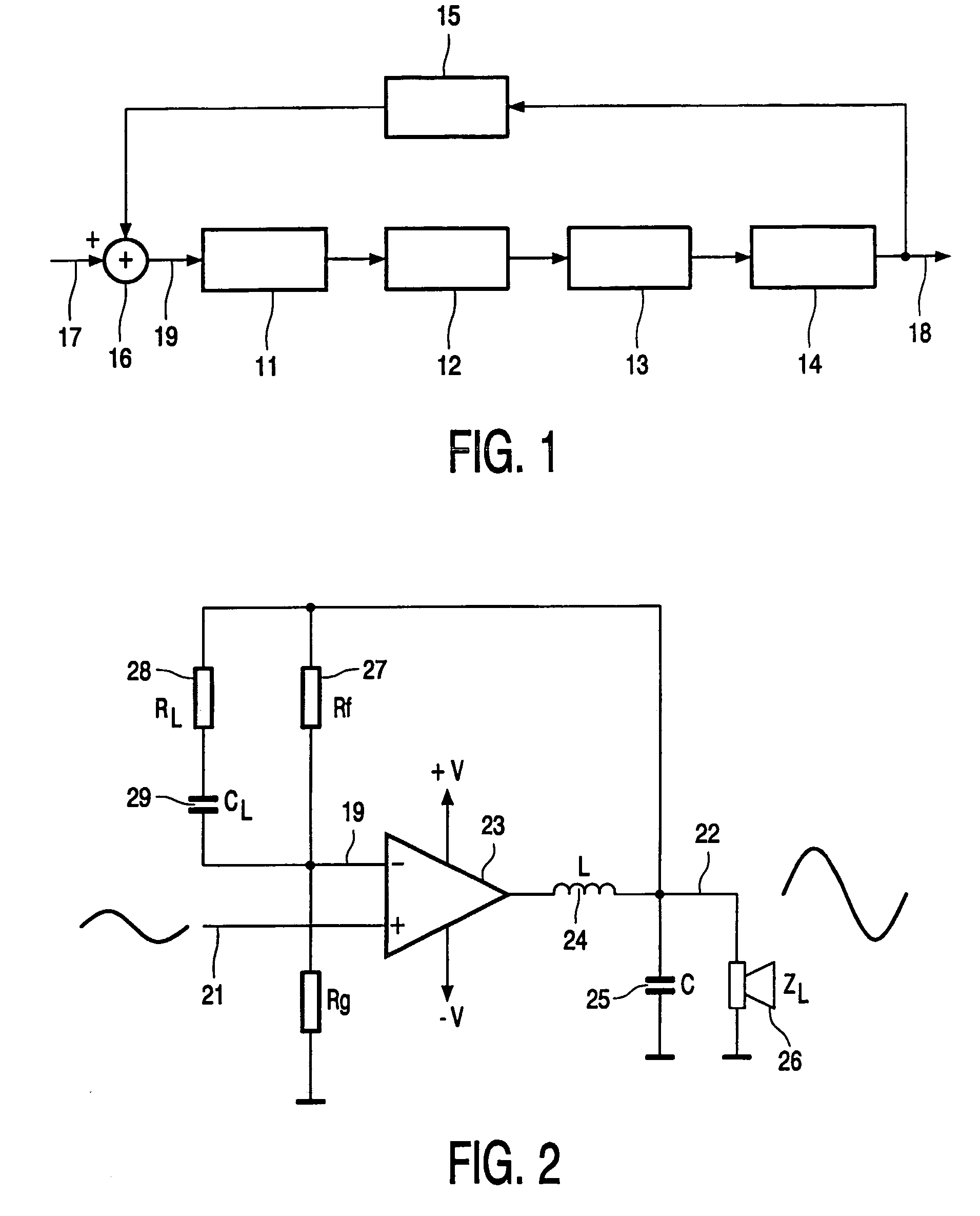
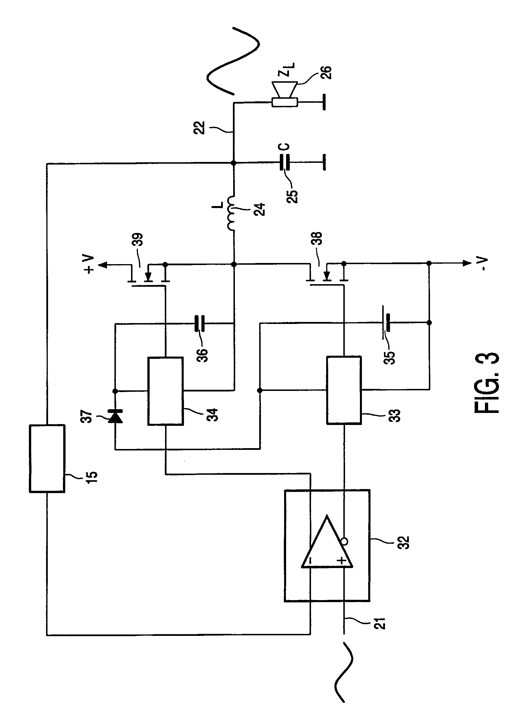
[0019]FIG. 1 shows a block diagram of a switching power amplifier. The amplifier has an input circuit 11 which receives a signal from a summing node 16 at a hysteresis-free input 19. The input circuit 11 is coupled to a driver element 12 for driving a switching power stage 13. The output of switching power stage 13 is a block wave signal having a frequency well above the operational frequency range of the electrical signal to be amplified. The block wave signal is coupled to a low-pass filter 14, which removes the high frequency block wave and results in a power output signal 18. A control circuit 15 provides a feedback loop from the power output signal 18 to the summing node 16 at the input. The summing node further receives the electrical input signal 17 which is to be amplified. Some delay is present in the elements 11, 12, 13 of the amplifying chain due to the physical nature of the circuits used, e.g., semiconductors. The control circuit 15 is provided with oscillation feedback...


PUM


Abstract

A switching power amplifier of class D has a switching stage for generating a block wave signal by alternately switching the block wave signal between supply voltages. A filter (24, 25) generates a power output signal (22) corresponding to an input signal to be amplified, which is coupled to a linear input (19) that is free of hysteresis. A control circuit (27, 28, 29) provides feedback between the output power signal and the linear input for controlling both the gain in the operational frequency range and also the alternately switching of the switching stage. Hence, the amplifier oscillates controlled via the same feedback loop that also controls the operational behavior of the amplifier, resulting in low output impedance and low distortion.

Description

BACKGROUND OF THE INVENTION[0001]1. Field of the Invention[0002]The invention relates to a power amplifier for amplifying an electric signal in an operational frequency range, the power amplifier comprising switching means for generating a block wave signal by alternately switching the block wave signal to a first supply voltage or a second supply voltage, filter means for generating a power output signal by low-pass filtering the block wave signal, input means for receiving the electric signal and driving the switching means, and a control circuit coupled to the output power signal and the input means for controlling the power amplifier.[0003]2. Description of the Related Art[0004]A switching power amplifier is known from U.S. Pat. No. 6,297,692. This patent describes pulse modulation amplifiers, also called pulse-width modulation amplifiers or class D amplifiers. In such amplifiers, there is an input stage for receiving an electrical input signal to be amplified, a modulating / swit...

Claims


Application Information

Patent Timeline
IPC IPC(8): H03F3/217H03F1/32H03F3/45
CPCH03F1/3211H03F3/2171H03F3/45085H03F2203/45648H03F2200/351H03F2200/78H03F2200/03
Inventor PUTZEYS, BRUNO JOHAN GEORGES
Owner KONINKLIJKE PHILIPS ELECTRONICS NV
Why Eureka
Try Eureka