
Method and system for area efficient charge-based capacitance measurement

a charge-based capacitance and area-efficient technology, applied in the field of semiconductor testing, can solve the problems of large waste of silicon area, excessively large silicon area required for all these probe pads, and large cost of large silicon area, so as to reduce the number of total pins and minimize the silicon area of the probe pads.

Active Publication Date: 2006-09-12
BELL SEMICON LLC
View PDF3 Cites 18 Cited by
  • Summary
  • Abstract
  • Description
  • Claims
  • Application Information

AI Technical Summary

Benefits of technology

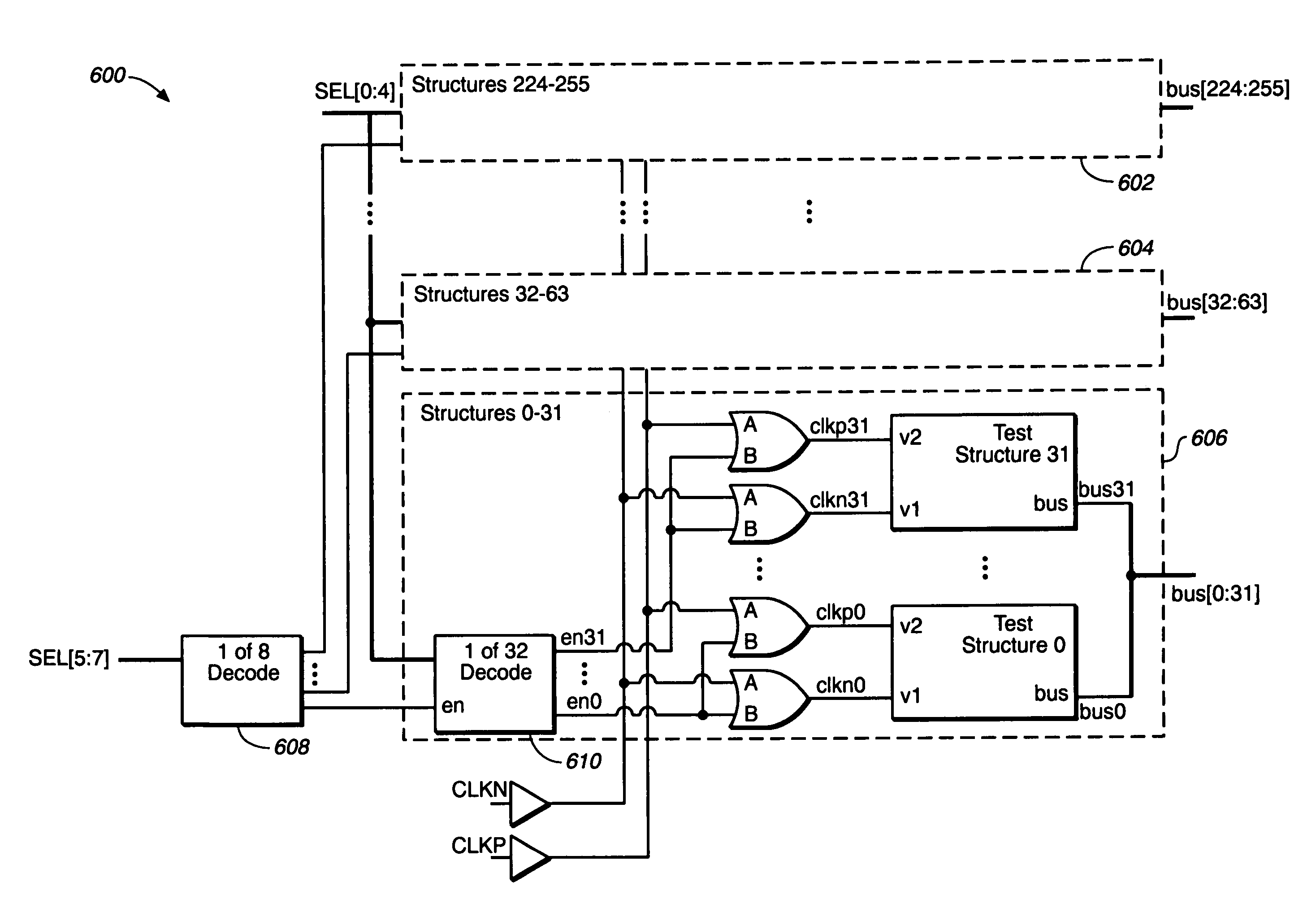
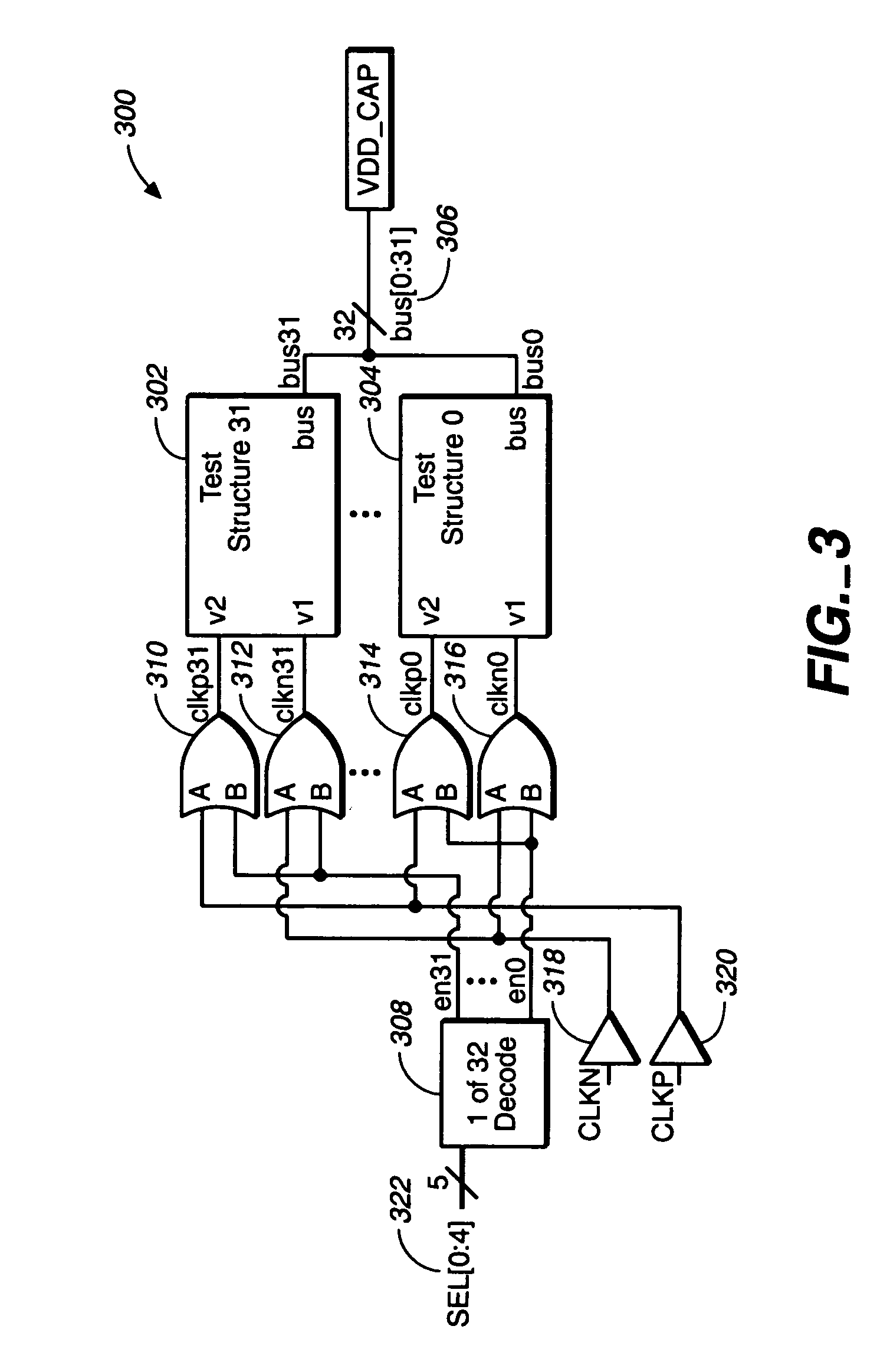
[0010]In an exemplary aspect of the present invention, a structure block for a chip capacitance measurement system is provided. The structure block includes several test structures coupled to a corresponding reference capacitance structure and a decode logic block. Each test structure includes a first PMOS transistor, a first NMOS transistor, and a test output. The decode logic block coupled to the several test structures selects a desirable test structure for test from the several test structures. A reference structure is identical to the test structures except it has no unique interconnect and is shared by several test structures. A current meter may be coupled to the structure block to measure currents in the desirable test structure and the reference structure. Consequently, a capacitance of the corresponding test capacitance structure is assessed through a conventional CBCM method. The assessed capacitance may include a parasite capacitance between two metallic layers, a metallic layer and a substrate, or the like. Additionally, the structure block includes a single output pin for busing the test outputs from the several test structures. The single output pin is coupled to a power source such as VDD_CAP. In this manner, the number of total pins may be reduced and, thus, the silicon area for probe pads may be minimized.

Problems solved by technology

However, probe pad sizes and spacing are huge relative to the area required to implement the pseudo-inverters and interconnect structure, so this is a tremendous waste of silicon area.
Large silicon area is very costly even for test chip work.
In such case, the silicon area required for all these probe pads is still excessively large.
If the number of the test structures is limited to reduce the silicon area less than a prescribed or assigned area, the test chip may result in incomplete characterization.

Method used


Image

  • Method and system for area efficient charge-based capacitance measurement
  • Method and system for area efficient charge-based capacitance measurement
  • Method and system for area efficient charge-based capacitance measurement

Examples


Embodiment Construction

[0020]Reference will now be made in detail to the presently preferred embodiments of the invention, examples of which are illustrated in the accompanying drawings.

[0021]The present invention is directed to a system having test structures to measure interconnect capacitance to calibrate various extraction tools which typically require excessively large silicon area. The system may include several structure blocks each of which include multiple test structures. In order to reduce a total number of pins and minimize silicon area for probe pads, a single output pin is utilized per structure block. Several outputs for the multiple test structures may be bused into the single output pin through a single serial bus. The single output pin is suitable for being returned to a power supply such as VDD_CAP, and the like. As mentioned above, some prior art requires multiple output pins for several test structures, which increases the silicon area and, thus, increase the area penalty associated w...


PUM


Abstract

The present invention is directed to a system for area efficient charge-based capacitance measurement requiring a minimum silicon area for probe pads. A structure block for the system includes several test structures coupled to a target test capacitance structure, a reference structure, and a logic block. Each test structure is coupled to a corresponding test capacitance structure. The logic block coupled to the several test structures selects a desirable test structure from the several test structures. The system may include several structure blocks and an additional logic block to select a desirable structure block. Each structure block includes a single output pin for busing each test output from the several test structures. In this manner, the silicon area may be minimized through reduction of the number of total pins and probe pads required.

Description

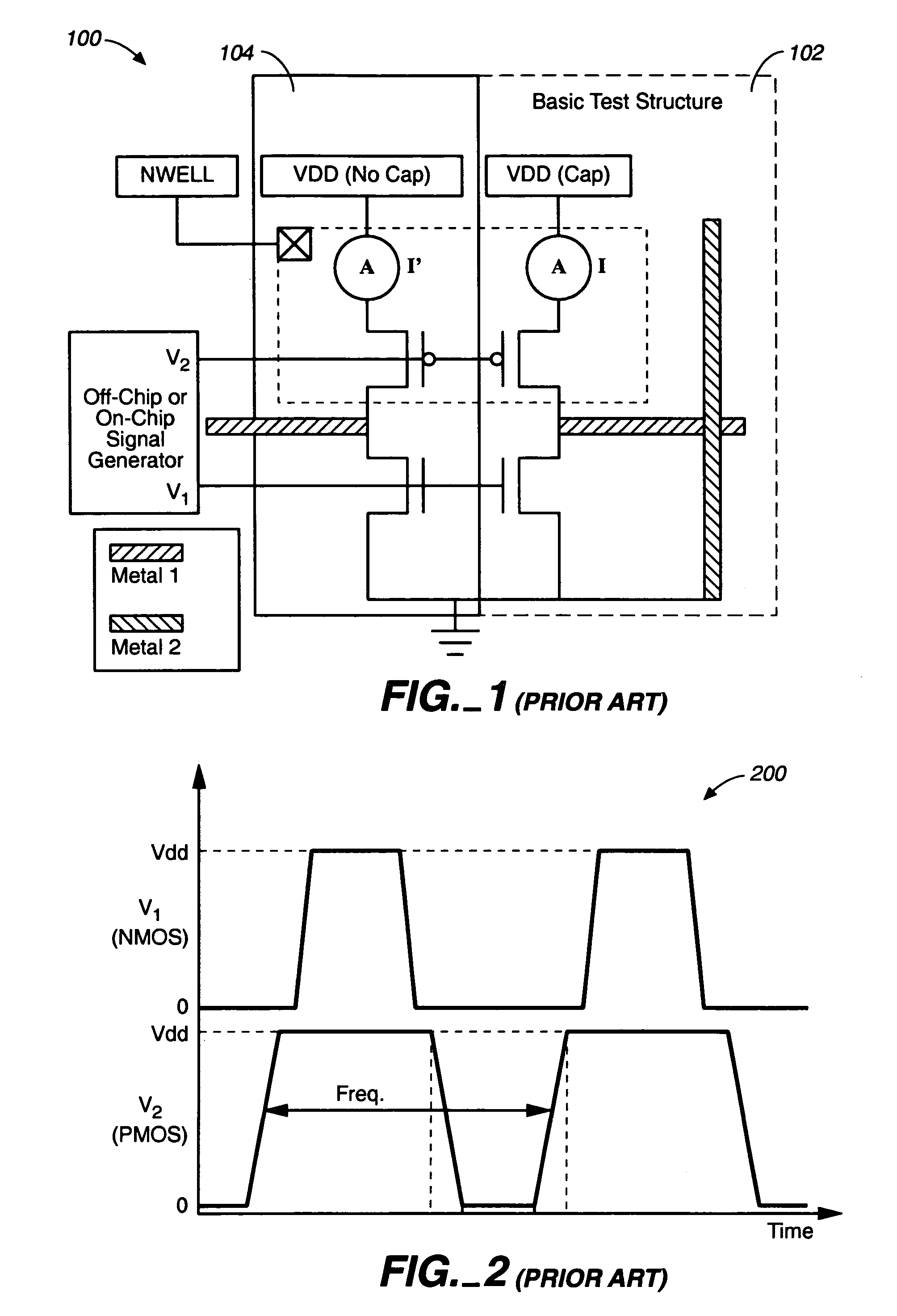
FIELD OF THE INVENTION[0001]The present invention generally relates to the field of semiconductor testing, and particularly to a system for area efficient charge-based capacitance measurement (CBCM) in semiconductor testing.BACKGROUND OF THE INVENTION[0002]The performance of today's deep sub-micron semiconductor processes is becoming more dependent upon the parasitic capacitances of metal interconnects. The parasitic capacitances are formed due to the coupling between a metallic interconnect and a substrate or between pairs of metallic interconnects. In order to properly calibrate CAD tools which extract interconnect capacitances from completed layouts, test chips are often designed and fabricated with many test structures composed of accurately controlled interconnect geometries. When the capacitance of these various structures is measured on the actual silicon, they are compared with the extracted results to assess the degree of correlation. If discrepancies exist, the information...

Claims


Application Information

Patent Timeline
Patent Type & Authority Patents(United States)
IPC IPC(8): G01R27/26
CPCG01R31/2884G01R31/2856
Inventor BACH, RANDALLSATHER, JEFFREY
Owner BELL SEMICON LLC
Learn More