Method for peeling off semiconductor element and method for manufacturing semiconductor device

a technology of peeling off semiconductor elements and manufacturing methods, which is applied in the direction of semiconductor devices, electrical devices, transistors, etc., can solve the problems of reducing the thickness of glass substrates, limiting the formation of larger voids, and the heat resistance of plastic substrates not high enough to withstand heat treatment, so as to achieve the effect of more volume and easy formation

Inactive Publication Date: 2006-09-12
SEMICON ENERGY LAB CO LTD
View PDF11 Cites 24 Cited by
  • Summary
  • Abstract
  • Description
  • Claims
  • Application Information

AI Technical Summary

Benefits of technology

[0010]According to the invention, a first base layer having recessed portions and projective portions is formed on a substrate and a second base layer is formed thereon. The form of the recessed portions of the first base layer is determined so that voids are formed inside the second base layer at least on the recessed portions of the first base layer. The narrower and deeper opening portions of the recessed portions are, the voids can be formed easier and the voids occupy more volume in the recessed portions.
[0017]When the peel-off is conducted, it is not necessary to irradiate laser beam directly to the semiconductor element, and either to perform heat treatment which adversely affects the properties of the semiconductor element. Accordingly, the semiconductor layer can be kept with little deterioration. Internal stresses of the second base layer and the semiconductor layer can be lowered due to the voids, and stress migration during manufacturing steps of the semiconductor element can also be improved.
[0018]According to the invention, by using an insulating layer having recessed portions and projective portions, the size, form and layout of a void can be easily optimized, and physical forces required for peeling off or processing time required for facilitating the peel-off can be reduced. Thus, the semiconductor element can be peeled off with little deterioration. In addition, by using an insulating layer having recessed portions and projective portions, the size, form and layout of a void can be easily optimized for etching. Further, physical forces required for peeling off as well as processing time required for facilitating the peel-off can be reduced. Thus, the semiconductor element can be peeled off with little deterioration.
[0019]As described above, by using an insulating layer having recessed portions and projective portions, the size, form and layout of a void can be easily optimized, and physical forces required for peeling off or processing time required for facilitating the peel-off can be reduced, hence the semiconductor element can be peeled off with little deterioration. Moreover, by using an insulating layer having recessed portions and projective portions, which enables to optimize the size, form and layout of a void, an etchant can be effectively diffused inside the void and the inner wall of the void can be enlarged. Accordingly, processing time required for etching can be reduced. In the case where the semiconductor element is physically peeled off after etching, the physical forces required for the peel-off can also be reduced, and thus the semiconductor element can be peeled off with little deterioration. Further, according to the invention, when the peel-off is performed, it is not necessary to irradiate laser beam directly to the semiconductor element, nor to perform heat treatment which adversely affects the properties of the semiconductor element. Therefore, a semiconductor layer can be kept with little deterioration. In addition, internal stresses of the second base layer and the semiconductor layer can be lowered due to the void, and stress migration during manufacturing steps of the semiconductor element can also be improved.

Problems solved by technology

However, there is a limit in reducing the thickness of a glass substrate when the mechanical strength of the display panel is considered.
However, in many cases, the heat resistance of a plastic substrate is not high enough to withstand a heat treatment during manufacturing steps of a semiconductor element.
However, since the voids are formed by photo etching according to the peeling method disclosed in Patent Document 1, there is a limit in making larger voids.
Therefore, it is not possible to appropriately enlarge the voids in order to reduce the time required for dissolution and fracture of a layer on which the voids are formed or to reduce the stress of a semiconductor layer when peeled off.
Moreover, although a peeling method of a single crystalline semiconductor layer is disclosed in Patent Document 1, there is no specific description of a peeling method of a thin film semiconductor element on an insulating surface by the use of voids.

Method used


Image

  • Method for peeling off semiconductor element and method for manufacturing semiconductor device
  • Method for peeling off semiconductor element and method for manufacturing semiconductor device
  • Method for peeling off semiconductor element and method for manufacturing semiconductor device

Examples


embodiment mode 1

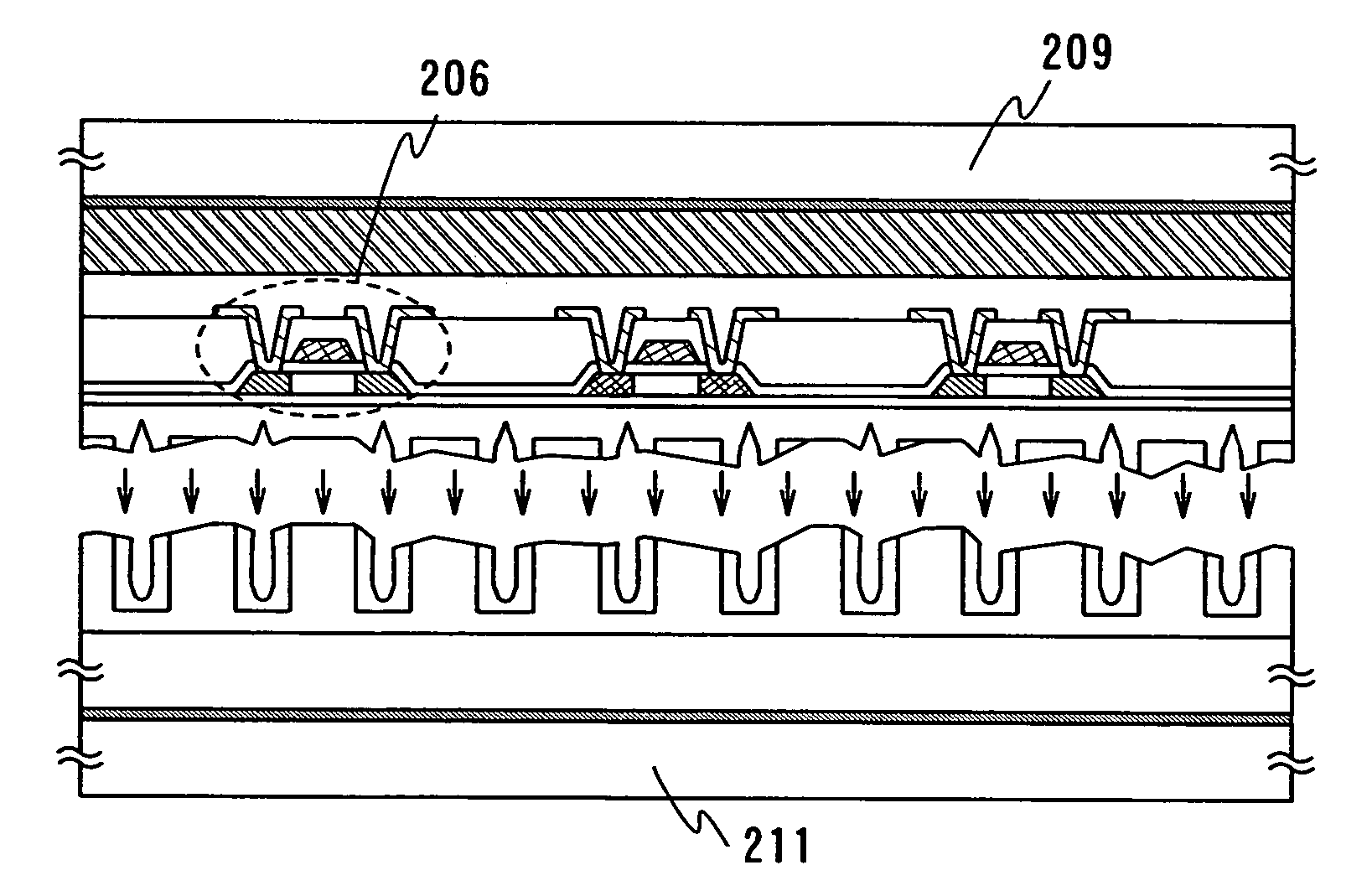
[0035]Explanation is hereinafter made on a manufacturing method of a semiconductor device by using a peeling method according to the invention.

[0036]First, a first base layer 201 having recessed portions and projective portions is formed on a first substrate 200 as shown in FIG. 2A. The first substrate 200 can be formed of a material which is capable of withstanding a heat treatment in subsequent steps. For example a quartz substrate, a silicon substrate, a glass substrate such as of barium borosilicate glass or aluminum borosilicate glass, a metal substrate, stainless substrate and the like are available.

[0037]In this embodiment mode, a silicon oxide layer is used for the first base layer 201. However, a material for the first base layer 201 is not limited to this, and an insulating layer such as silicon nitride layer and silicon nitride oxide layer or a metal layer such as W and Mo may also be used. A method for forming the recessed portions and projective portions will be describ...

embodiment mode 2

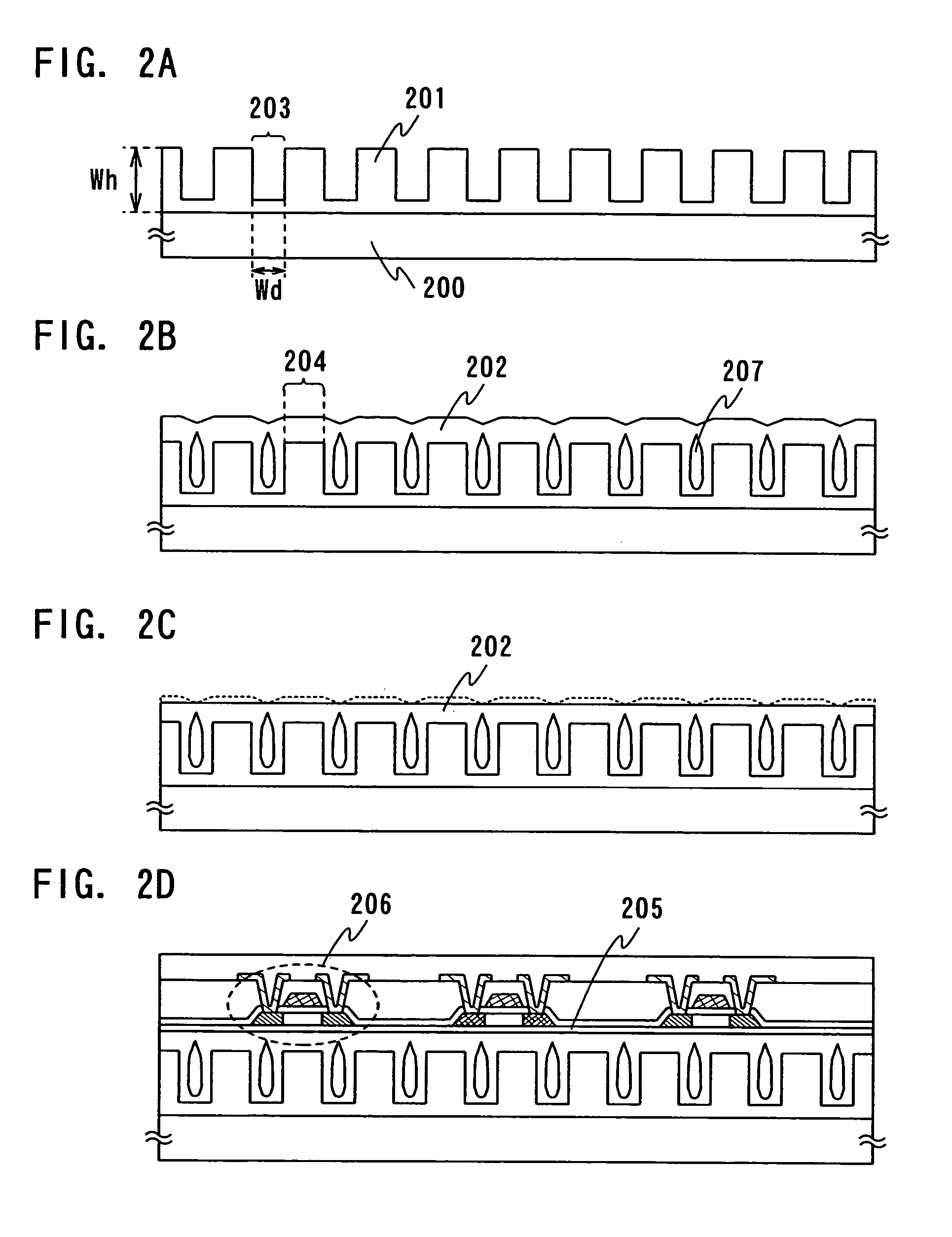
[0076]Explanation will be hereinafter made on a manufacturing method of a first base layer which has recessed portions and projective portions and is formed of an insulating layer. Needless to say, the manufacturing method and structure of the first base layer described below is just an example, and the invention is not limited this.

[0077]First, a first insulating layer 602 is formed on a first substrate 601 as shown in FIG. 8A. A silicon oxynitride layer is used for the first insulating layer 602 in this embodiment mode, though the invention is not limited to this and other insulating layer can be used as long as it has high etching selectivity relative to a second insulating layer formed thereon. In this embodiment mode, SiH4 and N2O are deposited by CVD to have a film thickness of 50 to 200 nm to form the first insulating layer 602. The first insulating layer 602 may have either a single layer structure or a laminated structure of a plurality of insulating layers.

[0078]Next, a se...

embodiment mode 3

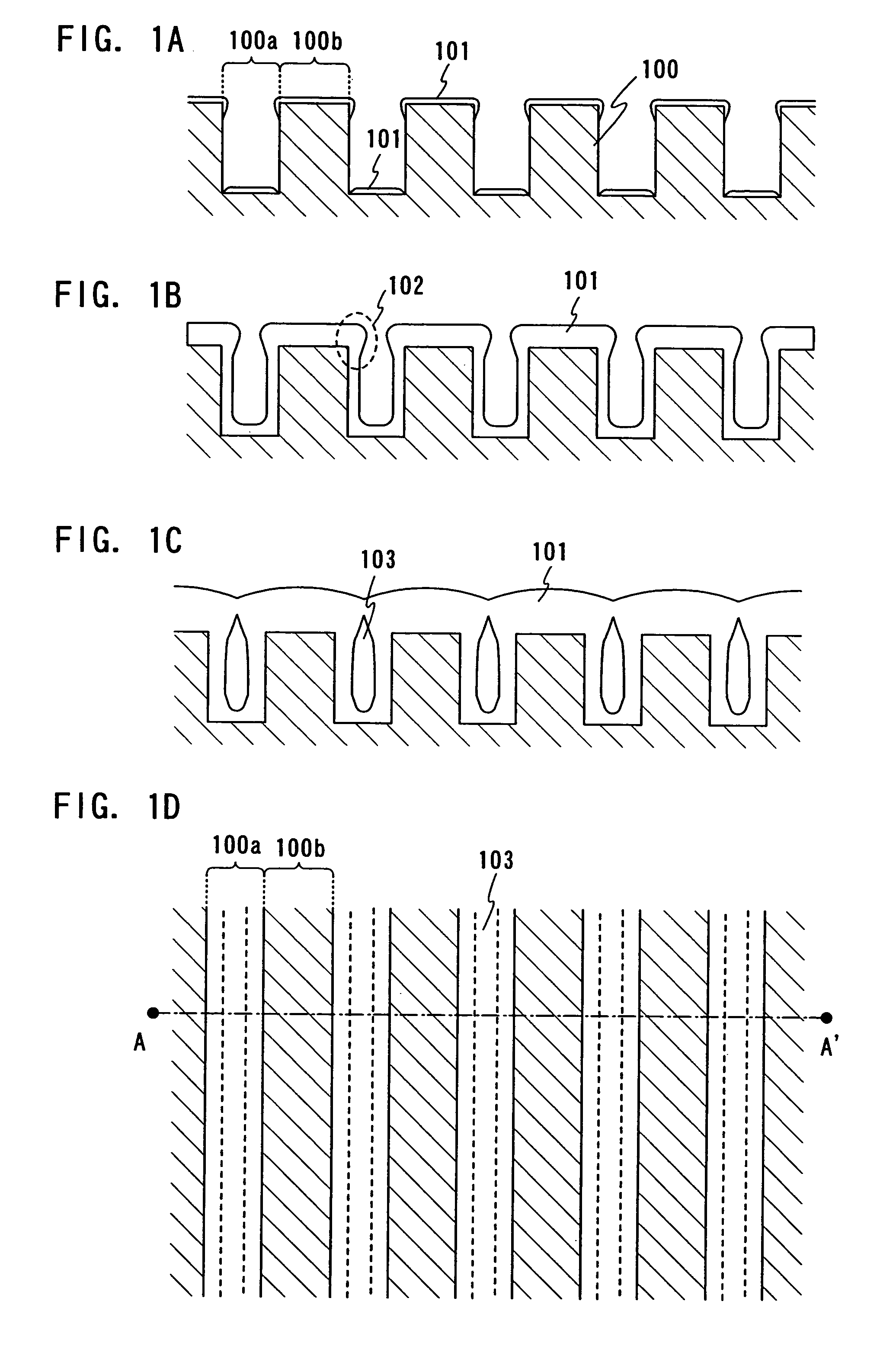
[0085]Explanation will be hereinafter made on a peeling method of the invention when using a metal layer for a first base layer.

[0086]First, a first base layer 801 having recessed portions and projective portions is formed on a first substrate 800 as shown in FIG. 10A. As well as the case shown in Embodiment Mode 1, in which an insulating layer is used for a first base layer, the first substrate 800 can be formed of a material which is capable of withstanding a heat treatment in subsequent steps. The first base layer 801 is formed of W (tungsten) in this embodiment mode. A metal layer is deposited on the first substrate 800 by sputtering and patterned in order to form the first base layer 801. The first base layer 801 may have either a single layer structure or a laminated structure of metal layers.

[0087]The form of the recessed portions and projective portions can be appropriately determined by a designer in accordance with a deposition method and a peeling method. In this embodime...


PUM


Abstract

A method for peeling off a thin film semiconductor element over an insulating surface by using a void, and a method for manufacturing a semiconductor device by transferring the peeled semiconductor element. According to the peeling method of the invention, a first base layer having a plurality of recessed portions is formed over a substrate, and a second base layer having a plurality of voids is formed on the recessed portions of the first base layer. On the second base layer, a third base layer is formed and a semiconductor element is formed thereon. Then, by separating the second base layer at an intersecting surface with the voids, the semiconductor element is peeled off from the substrate.

Description

BACKGROUND OF THE INVENTION[0001]1. Field of the Invention[0002]The present invention relates to a method for peeling off a semiconductor element formed on an insulating surface and to a method for manufacturing a semiconductor device by using the peeling method.[0003]2. Description of the Related Art[0004]Portable electronic equipment typified by a mobile phone, an electronic notebook and the like require multiple functions such as sending and receiving e-mail, voice recognition, taking-in images by a small camera as well as a flat panel display for displaying images. On the other hand, reduction in size and weight of the portable electronic equipment is still sought for satisfying the user needs. Therefore, as many ICs having larger circuit scale and memory capacity as possible are required to be mounted on the narrow space of the portable electronic equipment. It is an essential part to make a flat panel display to be mounted as thin and light as possible in order to achieve the ...

Claims


Application Information

Patent Timeline
Patent Type & Authority Patents(United States)
IPC IPC(8): H01L21/302H01L21/461H01L21/68H01L21/77H01L21/84H01L27/12H01L29/786
CPCH01L21/6835H01L27/1214H01L27/1266H01L29/78603H01L2924/19041H01L2221/68318H01L2221/68359H01L2221/68368
Inventor TAKAYAMA, TORUARAI, YASUYUKI
Owner SEMICON ENERGY LAB CO LTD
Why Eureka
Try Eureka