Non-volatile memory and fabricating method thereof

a non-volatile memory and fabricating method technology, applied in the field of semiconductor devices, can solve the problems of affecting the ultimate reliability of the device and the performance of the device, and achieve the effects of preventing any adverse effects on device performance, reducing line resistance in the source/drain region, and improving short channel

Active Publication Date: 2006-09-05
POWERCHIP SEMICON MFG CORP
View PDF1 Cites 7 Cited by
  • Summary
  • Abstract
  • Description
  • Claims
  • Application Information

AI Technical Summary

Benefits of technology

[0032]In the present invention, the line resistance in the source / drain region is reduced by forming the doped metal silicide layer under the control gate. Furthermore, through a heating process, the dopants inside the doped metal silicide layer will diffuse into the underlying substrate to form the source / drain region. Thus, abnormal electrical punch through between adjacent source / drain regions due to over-expansion of the source / drain regions is prevented so that a better short channel effect is obtained. In addition, using a metallic substance to form the control gate of a memory also prevents any adverse effects on device performance due to the diffusion of dopants into the tunneling oxide layer.

Problems solved by technology

In some cases, some of the dopants may diffuse into the surrounding dielectric layer and seriously affect the ultimate reliability of the device.
Hence, the performance of the device will also be affected.

Method used


Image

  • Non-volatile memory and fabricating method thereof
  • Non-volatile memory and fabricating method thereof
  • Non-volatile memory and fabricating method thereof

Examples


Embodiment Construction

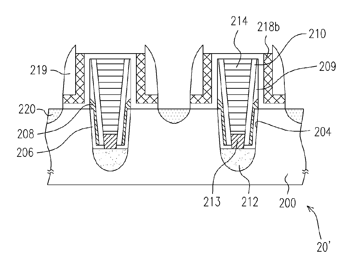
[0037]Reference will now be made in detail to the present preferred embodiments of the invention, examples of which are illustrated in the accompanying drawings. Wherever possible, the same reference numbers are used in the drawings and the description to refer to the same or like parts.

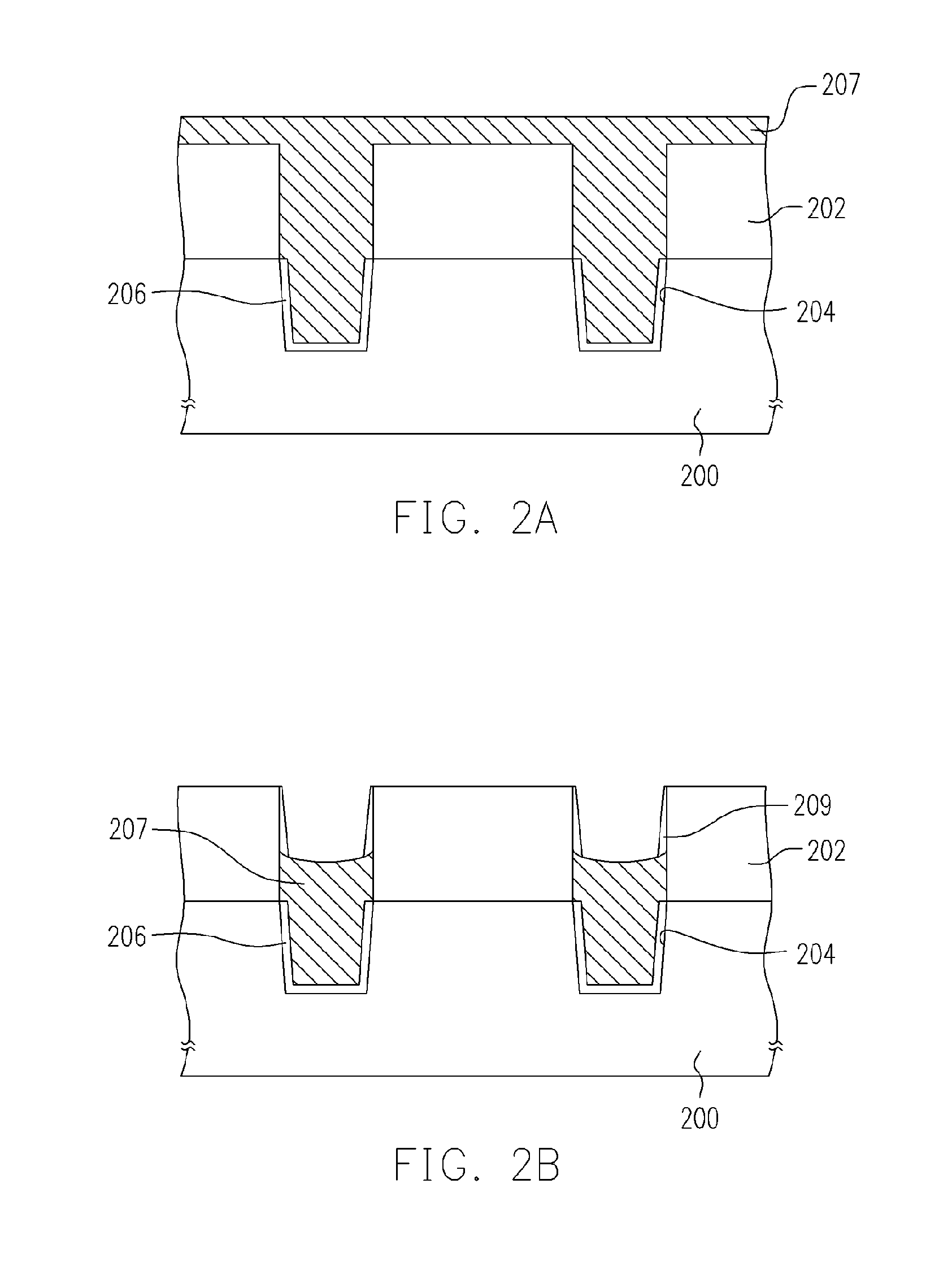
[0038]FIGS. 2A through 2G are schematic cross-sectional views showing the steps for fabricating a non-volatile memory according to one embodiment of the present invention. First, as shown in FIG. 2A, a substrate 200 is provided. Then, a patterned mask layer 202 is formed over the substrate 200. The patterned mask layer 202 is fabricated using silicon nitride, for example. Thereafter, using the patterned mask layer 202 as a mask, an etching operation is carried out to form a trench 204 in the substrate 200. A dielectric layer 206, serving as a tunneling oxide layer, is formed on the surface of the trench 204. The dielectric layer 206 is fabricated using silicon oxide, for example. The dielectric layer...


PUM

PropertyMeasurementUnit
thicknessaaaaaaaaaa
non-volatile aaaaaaaaaa
conductiveaaaaaaaaaa

Abstract

A method of fabricating a non-volatile memory is provided. A substrate having a trench therein for forming a trench device is provided. Then, a doped metal silicide layer is formed on the substrate in the trench. A heating process is performed to form a source/drain area in the substrate under the doped metal silicide layer. Thereafter, a first conductive layer is formed on the doped metal silicide layer to fill up the trench.

Description

CROSS-REFERENCE TO RELATED APPLICATION[0001]This application claims the priority benefit of Taiwan application serial no. 94120135, filed on Jun. 17, 2005. All disclosure of the Taiwan application is incorporated herein by reference.BACKGROUND OF THE INVENTION[0002]1. Field of the Invention[0003]The present invention relates to a semiconductor device and a fabricating method thereof. More particularly, the present invention relates to a non-volatile memory and a fabricating method thereof.[0004]2. Description of the Related Art[0005]Memory is a semiconductor device designed to store data or parameters. With the production of increasingly powerful microprocessors, the size of the software programs that are operated by memory increases correspondingly. As a result, the demand for a high storage capacity memory is getting higher and higher. The challenge of producing memory with a larger storage capacitor in accordance with this trend is now the force driving the techniques and process...

Claims


Application Information

Patent Timeline
Patent Type & Authority Patents(United States)
IPC IPC(8): H01L29/788
CPCH01L21/28273H01L29/42336H01L27/11556H01L27/115H01L29/40114H10B69/00H10B41/27
Inventor WANG, PIN-YAOLAI, LIANG-CHUAN
Owner POWERCHIP SEMICON MFG CORP
Why Eureka
Try Eureka