Semiconductor device and method of manufacturing the same

Inactive Publication Date: 2006-08-15
SEMICON ENERGY LAB CO LTD
View PDF16 Cites 91 Cited by
  • Summary
  • Abstract
  • Description
  • Claims
  • Application Information

AI Technical Summary

Benefits of technology

[0013]To achieve the above-described object, according to the present invention, when an element-formed layer is formed, the adhesiveness of a substrate and a semiconductor element is enhanced. On the contrary, after the element-formed layer is formed, the adhesiveness of the substrate and the semiconductor element is lowered.
[0043]Moreover, according to the present invention, the adhesive agent is formed over the substrate in advance, thereby enhancing the adhesiveness of the substrate and the element-formed layer including the integrated circuit in manufacturing. Therefore, it can be prevent the element-formed layer from peeling off the substrate while manufacturing. On the other hand, after the element-formed layer has been formed, the element-formed layer can easily be separated from the substrate, since the adhesive agent can be removed to reduce the adhesiveness of the substrate and the element-formed layer. In other words, the adhesiveness of the substrate and the element-formed layer can be controlled when a semiconductor device is manufactured.

Problems solved by technology

As a result, it becomes possible to manufacture a semiconductor element over a glass substrate, which has been impossible in the high temperature process.
However, it is extremely difficult to manufacture a semiconductor element over a flexible substrate such as plastic from a viewpoint of heat-resistance of a substrate, because much lower-temperature is necessary.
In the case of the method (1), there is a problem of a longer process time or high material cost of an etching material or a glass substrate, although a substrate is completely separated from a semiconductor element after forming the semiconductor element over the substrate.
Namely, there is a problem of peeling off while manufacturing a semiconductor element, although it is easier to perform separation with lower adhesiveness and higher film stress.
There is also difficulty in performing separation of a semiconductor element from a substrate after the semiconductor element is formed, although peeling-off of the semiconductor element does not occur in the middle of manufacturing the semiconductor element, if the adhesiveness is enhanced.

Method used


Image

  • Semiconductor device and method of manufacturing the same
  • Semiconductor device and method of manufacturing the same
  • Semiconductor device and method of manufacturing the same

Examples


embodiment mode 1

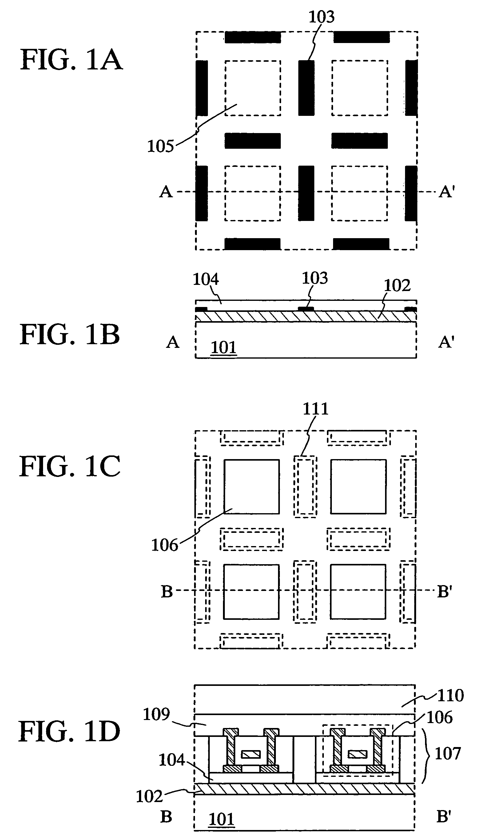
[0071]An embodiment mode of the present invention is described with reference to FIGS. 1A to 1D.

[0072]FIG. 1A is a top view of a substrate where an adhesive agent of the present invention is formed, whereas FIG. 1B is a cross-sectional view taken along a dotted line AA′ in FIG. 1A. Namely, an adhesive agent 103 is formed like an island to be in contact with a metal layer 102 formed on a substrate 101 as shown in FIG. 1B. Note that, the adhesive agent that is formed here can enhance the adhesiveness of the metal layer 102 and the oxide layer 104 to be formed next, since the adhesive agent is formed between the metal layer 102 and the oxide layer 104.

[0073]A quartz substrate, a glass substrate, or the like can be used for a material of the substrate 101. However, a plurality of substrates can be bonded together and used, in the case where the strength is not enough when an element-formed layer (including a TFT) formed over a substrate is separated from the substrate in a later step.

[0...

embodiment mode 2

[0088]An embodiment mode of the present invention is described with reference to FIGS. 14A to 14D.

[0089]FIG. 14A is a top view of a substrate where an adhesive agent of the present invention is formed, whereas FIG. 14B is a cross-sectional view taken along a dotted line AA′ in FIG. 14A. Namely, an adhesive agent 3103 is formed like an island to be in contact with a metal layer 3102 formed on a substrate 3101 as shown in FIG. 14B. Note that, the adhesive agent that is formed here can enhance the adhesiveness of the metal layer 3102 and the oxide layer 3104 to be formed next, since the adhesive agent is formed between the metal layer 3102 and the oxide layer 3104.

[0090]A quartz substrate, a glass substrate, or the like can be used for a material of the substrate 3101. However, a plurality of substrates can be bonded together and used, in the case where the strength is not enough when an element-formed layer (including plural integrated circuits) formed over a substrate is separated fr...

embodiment 1

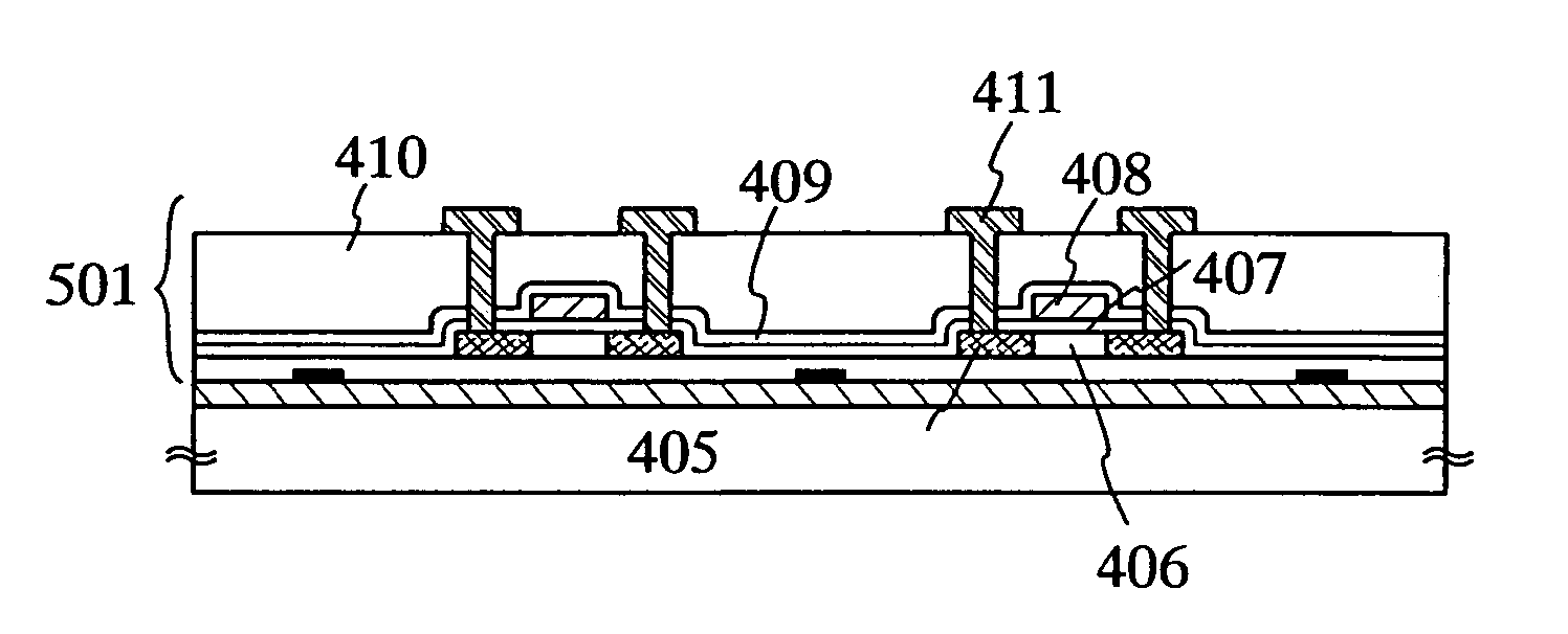
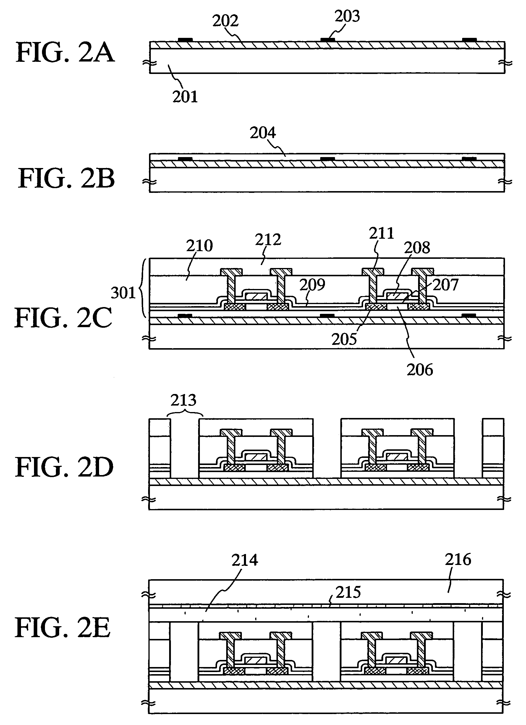
[0106]In this embodiment, a method for manufacturing including a transfer step of the present invention is described with reference to FIGS. 2A to 2E, and FIGS. 3A to 3D.

[0107]In FIG. 2A, a metal layer 202 is formed on a first substrate 201, and a plurality of adhesive agents 203 are formed thereon.

[0108]A glass substrate or a quartz substrate can be used as the first substrate 201 in this embodiment. Note that, a glass substrate containing barium borosilicate glass, alumino borosilicate glass, alumino silicate glass, or the like as a material is suitable. Representatively, a 1737 glass substrate (distortion point of 667° C.) manufactured by Corning Incorporated, AN 100 (distortion point of 670° C.) manufactured by Asahi Glass Co., Ltd., and the like are applicable. AN 100 is used in this embodiment.

[0109]A material of the metal layer 202 can be a single layer made of an element selected from the group consisting of: tungsten (W), molybdenum (Mo), technetium (Tc), rhenium (Re), ruth...


PUM


Abstract

To provide a method for manufacturing a semiconductor device including a transfer step that is capable of controlling the adhesiveness of a substrate and an element-formed layer in the case of separating the element-formed layer including a semiconductor element or an integrated circuit formed over the substrate from the substrate and bonding it to another substrate. An adhesive agent made of a good adhesiveness material is formed between the semiconductor element or the integrated circuit comprising plural semiconductor elements formed over the substrate (a first substrate) and the substrate, and thus it is possible to prevent a semiconductor element from peeling off a substrate in manufacturing the semiconductor element, and further, to make it easier to separate the semiconductor element from the substrate by removing the adhesive agent after forming the semiconductor element.

Description

BACKGROUND OF THE INVENTION[0001]1. Field of the Invention[0002]The present invention relates to a method for manufacturing a semiconductor device including a transfer step of a semiconductor element such as a thin film transistor (TFT) formed over a substrate, to another substrate.[0003]In addition, the present invention relates to a method for manufacturing a semiconductor device including a transfer step of an integrated circuit comprising a plurality of semiconductor elements (including a thin film transistor (TFT)) formed over a substrate, to another substrate.[0004]2. Description of the Related Art[0005]In recent years, various technical developments have been made about a semiconductor element represented by a thin film transistor (TFT) that is formed by using a semiconductor thin film (about from several nm to several hundred nm in thickness) formed over the same substrate.[0006]To secure characteristics of a semiconductor element, a certain level of high temperature is requ...

Claims


Application Information

Patent Timeline
IPC IPC(8): H01L21/00H01L21/30H01L21/46H01L21/336H01L21/77H01L21/84H01L27/12H01L29/423H01L29/49H01L29/786
CPCH01L27/1214H01L27/1266H01L29/42384H01L29/4908H01L29/78603H01L29/78675H01L29/66757H01L2221/68368H01L29/78621H01L2221/6835H01L27/1218H01L27/12
Inventor IMAI, KEITAROTAKAYAMA, TORUGOTO, YUUGOMARUYAMA, JUNYAOHNO, YUMIKO
Owner SEMICON ENERGY LAB CO LTD
Why Eureka
Try Eureka