Apparatus and method to reduce memory footprints in processor architectures

a processor architecture and memory footprint technology, applied in the direction of memory adressing/allocation/relocation, program loading/initiating, instruments, etc., can solve the problems of requiring more space for storage capacities on the chip, occupying more space on the integrated device than the processing components, and being expensive to produce, so as to reduce the memory footprint, the effect of reducing the cost and reducing the memory footprin

Inactive Publication Date: 2006-08-08
AVAGO TECH INT SALES PTE LTD
View PDF10 Cites 6 Cited by
  • Summary
  • Abstract
  • Description
  • Claims
  • Application Information

AI Technical Summary

Benefits of technology

[0014]The present invention provides for an apparatus and method for reducing the memory footprint on a processor intensive device such as a DSP, or the like. A piece of software (or algorithm) can be broken down into at least one controlling piece and at least one working piece. The controlling piece of software is allocated for storage (or execution) on an external storage device. This external storage device would likely consist of memory, which is lower in cost than the memory associated with a processor intensive device. The working piece of software is stored and executed on the processor intensive device (i.e., DSP). The invention also consists of a transfer mechanism for providing fast and efficient access to the controlling piece by the working piece, and vice versa.
[0015]In particular, the present invention provides for reducing the memory footprint in a dual processor construct, wherein a high-MIPS processor (such as a DSP), is used in conjunction with a low-MIPS general purpose microprocessor unit (MCU). When the DSP and MCU are integrated within a single device, a hardware mechanism can be added to allow the DSP to directly and efficiently access the less costly MCU memory. The present invention consists of a system in which this transfer mechanism is integrated—along with a restructuring of the software—in order to significantly reduce the required DSP memory footprint (and thereby the cost of the device), without impairing the performance of the device.

Problems solved by technology

Memory, however, often takes up more room on an integrated device than processing components, with higher storage capacities generally requiring more space on the chip.
This is often not favorable, as larger chip layouts are more expensive to produce, take up more room in compact devices, and often draw more power.
This is particularly true for processor intensive applications such as digital signal processing.
Whereas look-ahead caching schemes are commonly implemented on general purpose (MIPS) processors, such caching schemes are not well suited for DSP operations.
Due to the specialized nature of such DSP code—and its reliance on certain data that is often stored externally—it becomes difficult to cache code and / or data for look-ahead reference.
This traditional approach often does not significantly reduce the memory required by the DSP, as hand-optimization techniques can only reduce the length of the code by a certain degree.

Method used


Image

  • Apparatus and method to reduce memory footprints in processor architectures
  • Apparatus and method to reduce memory footprints in processor architectures
  • Apparatus and method to reduce memory footprints in processor architectures

Examples


Embodiment Construction

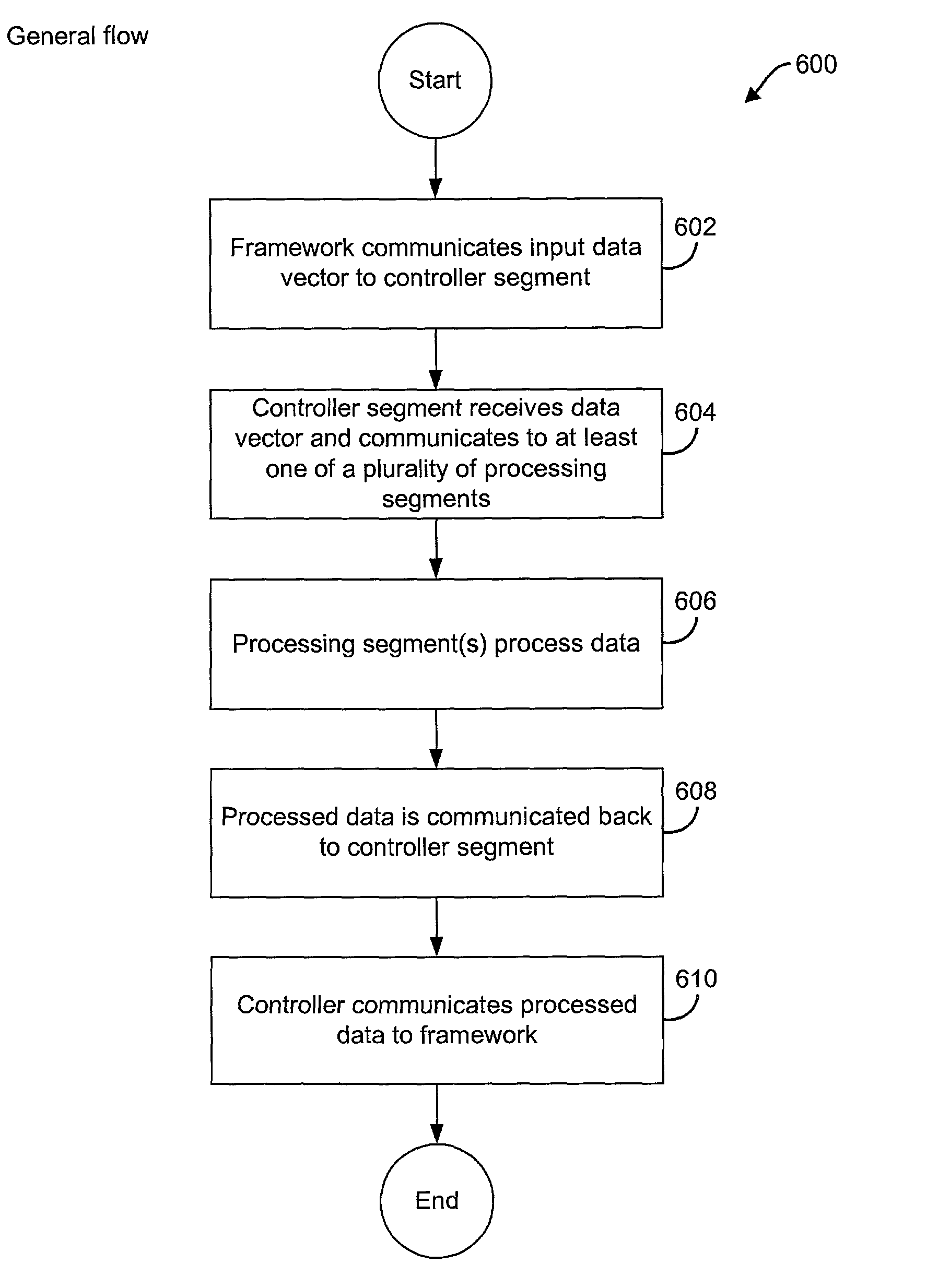
[0045]The present invention is described below in terms of certain preferred embodiments, and representative applications. The example apparatus and processing methods are intended to be used with any communication system that would benefit from having a reduced memory footprint, particularly in a processor intensive device such as a DSP. A reduction in memory on any type of device facilitates reduction of the overall size, cost, and complexity of the device, wherein DSPs are generally associated with more costly memory. Information and data might be stored and accessed from many types of external storage devices. Moreover, the information and data might be stored and processed in an associated processor having lower cost memory. The logical partitioning of the code into controlling pieces, working pieces, and data pieces, can also be advantageously applied to many other hardware architectures and structures.

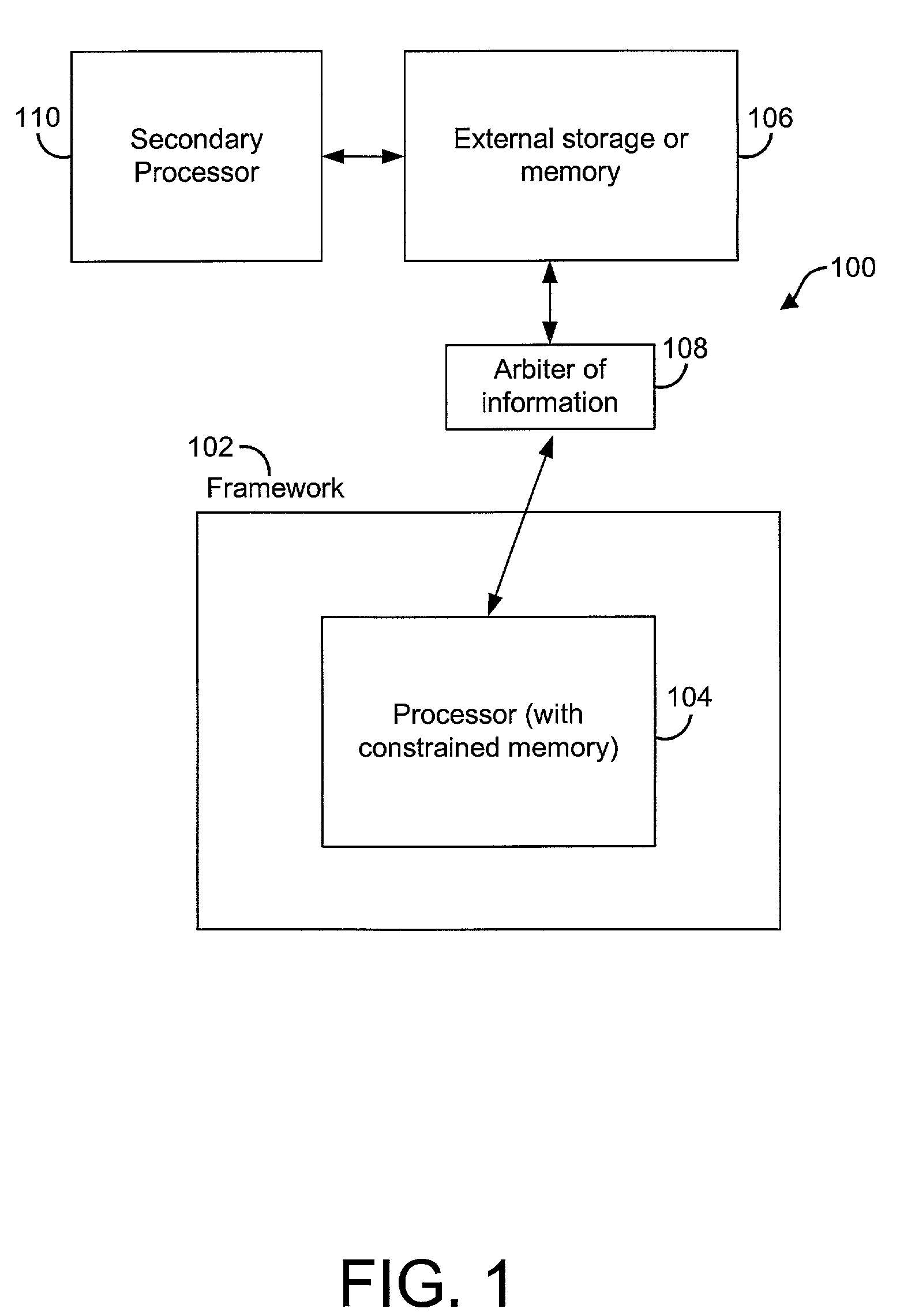
[0046]Referring to FIG. 1, a generalized block diagram 100 is shown of a fr...


PUM


Abstract

The present invention provides an apparatus and method to reduce the memory footprint of a processor architecture by structuring processor code to be stored in an external device, and transferring into the processor certain code and associated data as it is needed. The processor code or algorithm is divided into a controlling piece and a working piece. The controlling piece can be located on a low-MIPS, high memory-footprint device, whereas the working piece can be located on a high-MIPS, low memory-footprint device. The working piece can also be broken down into phases or segments, which are put in a data store. The segments are then transferred, on an as-needed basis along with associated data, from the store into the constrained memory of the low memory-footprint device. Transfer is facilitated by a segment manager which can be processed from the low-MIPS device, or alternatively from the high-MIPS device.

Description

RELATED APPLICATIONS[0001]This application claims priority of the following—U.S. provisional patent application having Ser. No. 60 / 269,378, entitled “Network Telephony Device,” filed Feb. 16, 2001, which is hereby incorporated by reference in its entirety.[0002]This application is related to the following—U.S. patent application having Ser. No. 10 / 032,667, entitled “Transferring Data Along With Code for Program Overlays,” filed on the same date herewith, which is hereby incorporated by reference in its entirety.FIELD OF THE INVENTION[0003]The present invention provides an apparatus and method to reduce the memory footprint of a processor architecture by structuring processor code to be stored in an external device, and transferring into the processor certain code and associated data as it is needed. In particular, the present invention can be readily applied to a network telephone device or the like.BACKGROUND OF THE INVENTION[0004]Ethernet networks and the like for providing data c...

Claims


Application Information

Patent Timeline
Patent Type & Authority Patents(United States)
IPC IPC(8): G06F12/00G06F9/445
CPCG06F9/44557G06F9/44521
Inventor HEMSING, CRAIGHYLANDS, DAVEJONES, ANDREWLI, HENRY W. H.PULLMAN, SUSAN
Owner AVAGO TECH INT SALES PTE LTD
Why Eureka
Try Eureka