Event based IC test system

a technology of ic test system and event, applied in the direction of testing circuit, instrument, program control, etc., can solve the problems of multiple clock domain devices untested, vector conversion consumes extensive time, and ic testing requires a different environment, so as to save engineering time and reduce the cost of testing semiconductor ics

Inactive Publication Date: 2006-08-08
ADVANTEST CORP
View PDF17 Cites 15 Cited by
  • Summary
  • Abstract
  • Description
  • Claims
  • Application Information

AI Technical Summary

Benefits of technology

[0014]It is another object of the present invention to provide a new tester architecture that allows IC design environment to extend from simulation to the physical testing of the designed integrated circuits (ICs).
[0015]It is a further object of the present invention to provide a new tester architecture that allows testing in design simulation environment, which saves engineering time and reduces cost of testing semiconductor ICs.
[0016]It is a further object of the present invention to provide a new tester architecture that eliminates vector processing steps in the conventional technology and greatly simplifies file requirements and pattern compilation process, thereby saving time, cost and avoiding errors in the vector conversion.
[0020]According to the present invention, the method and architecture of the test system allows testing and debug of ICs without diverting from the environment in which the IC was designed. As noted above, the traditional IC test systems require conversion of the design simulation data into a cyclized form, such as the WGL or STIL format. The new architecture avoids such conversion and uses design simulation data as-is. Thus, the method and apparatus of the present invention allow testing in the environment identical to the design simulation environment, which saves engineering time and reduces cost of testing semiconductor ICs.

Problems solved by technology

However, because of these limitations in today's test systems, IC testing requires a different environment than the original IC design and simulation environment.
From the user's point of view, the above limitations cause following problems: (i) vector conversion consumes extensive time, server and disk capacities, and is very error-prone, (ii) cyclization of vectors makes multiple clock domain devices untestable, and (iii) due to a finite number of resources such as timesets, waveform groups, timing generators, etc., there arises tester limitations.
Hence, it is a foreign environment from the original IC design environment and causes difficulties during testing and debug the ICs.
Converting the IC simulation vectors from the VCD format to the cyclized format is very time consuming, complex and error-prone.
This problem is further compounded by the fact that every tester has it's own unique and proprietary language and vector format (ex.
Subsequently, all this effort in vector conversion becomes extremely time consuming and costly.
This lengthy process also impedes the ability to process new or improved vectors quickly, thereby slowing the test and debug process.
Moreover, the very act of converting original IC simulation vectors into a tester's cyclized format endangers the accuracy of data.
This results in errors and test vectors that are no longer simulation-faithful.
All these problems result in additional time and cost.

Method used


Image

  • Event based IC test system
  • Event based IC test system
  • Event based IC test system

Examples


Embodiment Construction

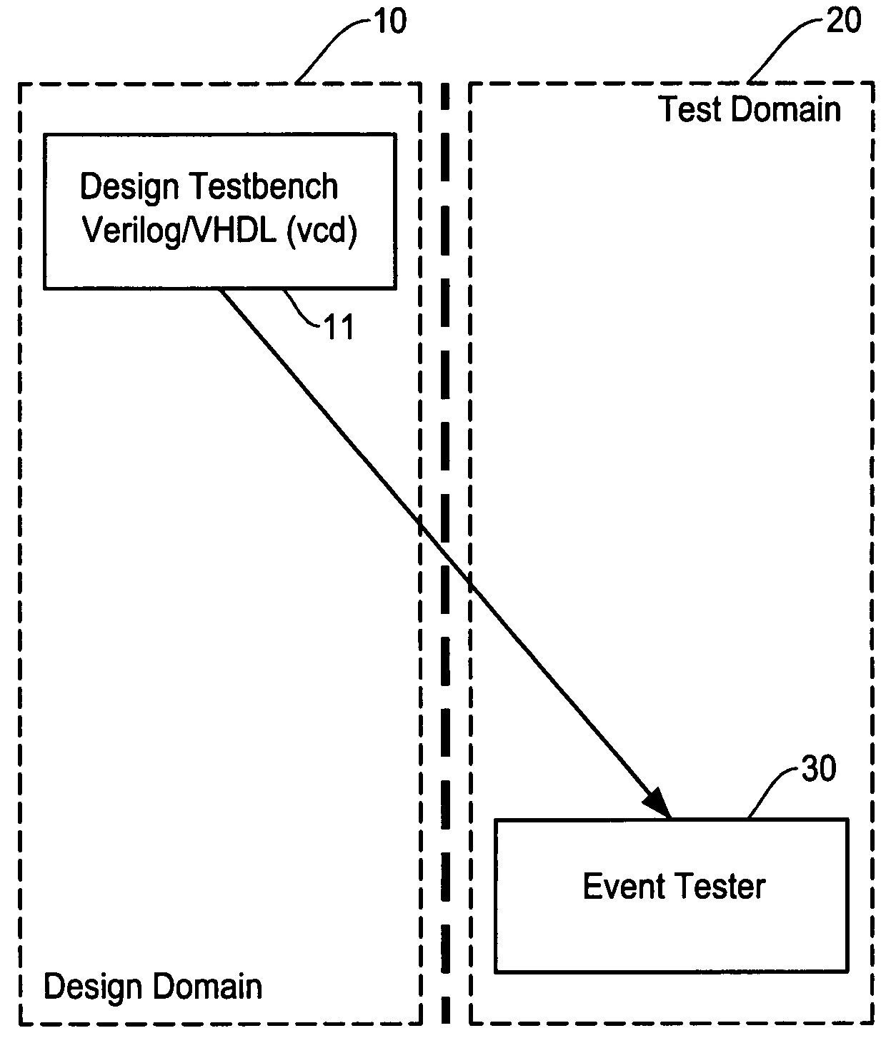
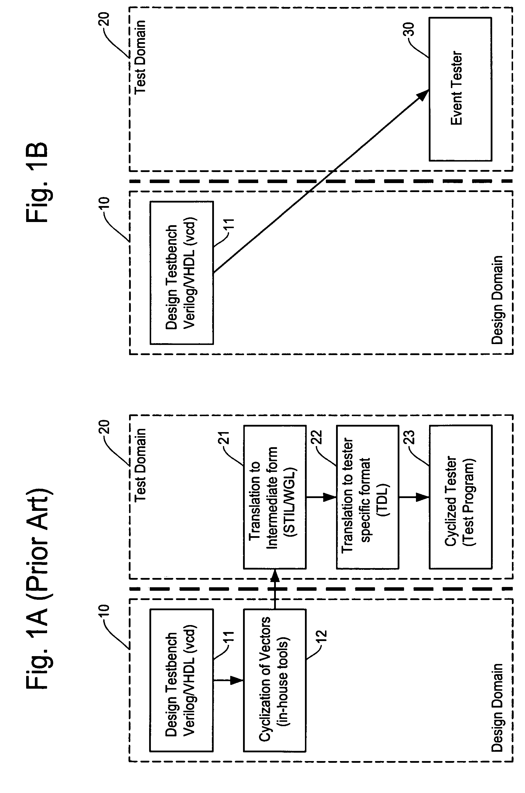
[0030]The present invention is now described in more detail with reference to the accompanying drawings. The problems mentioned above require a complete change in the environment and process as well as the architecture of the test system in use today. The solution needs a fundamental change that simplifies the testing and test system rather than adding yet more complexity to the already complicated process. For example, in principle, sophisticated software can be developed that ensures the correct vector translation from VCD to STIL. However, the basic problem of time, effort and cost due to the translation process still remains intact. Hence, the problem should be solved not by developing more sophisticated software, but by eliminating the need for vector translation itself.

[0031]In other words, the IC testing environment should be the same as the original IC design environment; engineers should not be required to change their simulation testbenches into ATE cyclized format, and VC...


PUM


Abstract

An event based test system for testing an IC device under test (DUT) designed under an automatic electronic design (EDA) environment. The event based test system includes an event memory for storing event data derived directly from simulation of design data for an intended IC in the EDA environment where the event data to denote each event is formed with time index indicating a time length from a predetermined point and an event type indicating a type of change at an event, an event generation unit for generating test vectors based on the event data where waveform of each vector is determined by the event type and a timing of the waveform is determined by accumulating the time index of previous events, and means for supplying test vectors to the DUT and evaluating response outputs of the DUT at predetermined timings.

Description

FIELD OF THE INVENTION[0001]This invention relates to a design and architecture of a new type of semiconductor IC test system, and more particularly, to an event based IC test system in which test data is utilized in an event form thereby enabling a direct use of design simulation data produced in an electronic design automation (EDA) environment.BACKGROUND OF THE INVENTION[0002]In testing semiconductor IC devices by a semiconductor IC test system (IC tester or tester), the basic procedure of functional testing of a semiconductor IC device contains creation of input (drive) stimulus for the IC device, application of these stimulus and comparison of the output of the IC device with expected results by strobing the outputs at predetermined times. Such input stimulus and strobes are collectively called a test pattern or test vector and are traditionally generated based on test data in a cyclized form. Such a traditional test system is sometimes called a cycle based test system or a cyc...

Claims


Application Information

Patent Timeline
Patent Type & Authority Patents(United States)
IPC IPC(8): G01R31/00G01R31/28G01R31/3181G01R31/3183G01R31/319
CPCG01R31/31813G01R31/318307G01R31/31928G01R31/31917G01R31/31919G01R31/318342
Inventor RAJSUMAN, ROCHITSUGAMORI, SHIGERUSAUER, ROBERT F.YAMOTO, HIROAKITURNQUIST, JAMES ALANPARNAS, BRUCE R.LE, ANTHONY
Owner ADVANTEST CORP
Why Eureka
Try Eureka