
Silica glass member for semiconductor and production method thereof

a technology of silicon glass and silicon, applied in glass tempering apparatus, crystal growth process, manufacturing tools, etc., can solve the problems of shortage of the life of the silicon glass member for semiconductors, lot of contamination of the semiconductor wafer, etc., and achieve the effect of reducing the purification

Inactive Publication Date: 2006-08-01
COVALENT MATERIALS CORP
View PDF7 Cites 4 Cited by
  • Summary
  • Abstract
  • Description
  • Claims
  • Application Information

AI Technical Summary

Benefits of technology

[0025]When the concentration of an OH group in the silica glass base material exceeds 50 ppm, a purifying effect produced by heat treatment is decreased.
[0033]When the heat-treating temperature is less than 1100° C., a purifying effect is decreased.

Problems solved by technology

However, these materials have the drawback that the concentration of metal impurities in these materials is high, so that a lot of impurities is discharged and there is therefore a lot of contamination to a semiconductor wafer during the course of the process.
Therefore, at a temperature above 1100° C., a deformation due to viscosity is caused, giving rise to unacceptable phenomena such as an expansion of a furnace core tube and a distortion of a wafer boat, leading to a shortage of the life of a silica glass member for semiconductors resultantly.

Method used


Image

  • Silica glass member for semiconductor and production method thereof
  • Silica glass member for semiconductor and production method thereof

Examples


example

[0037]First, silicon tetrachloride refined by distillation was vaporized and O2 (oxygen) gas was fed as a carrier gas to a flame of an oxyhydrogen burner to hydrolyze the silicon tetrachloride thereby depositing the synthetic silica powder on a target to make a porous body (soot). This porous body was heat-treated at 1300° C. in a reducing gas atmosphere (H2 gas: 25 vol % and N2 gas: 75 vol %) to obtain highly heat-resistant soot remelted synthetic silica glass.

[0038]A sample (20 mm×20 mm×2 mm) was cut out of the resulting highly heat-resistant remelted synthetic silica glass to measure the concentration of an OH group by an infrared absorption spectrum, to find that the concentration was 10 ppm.

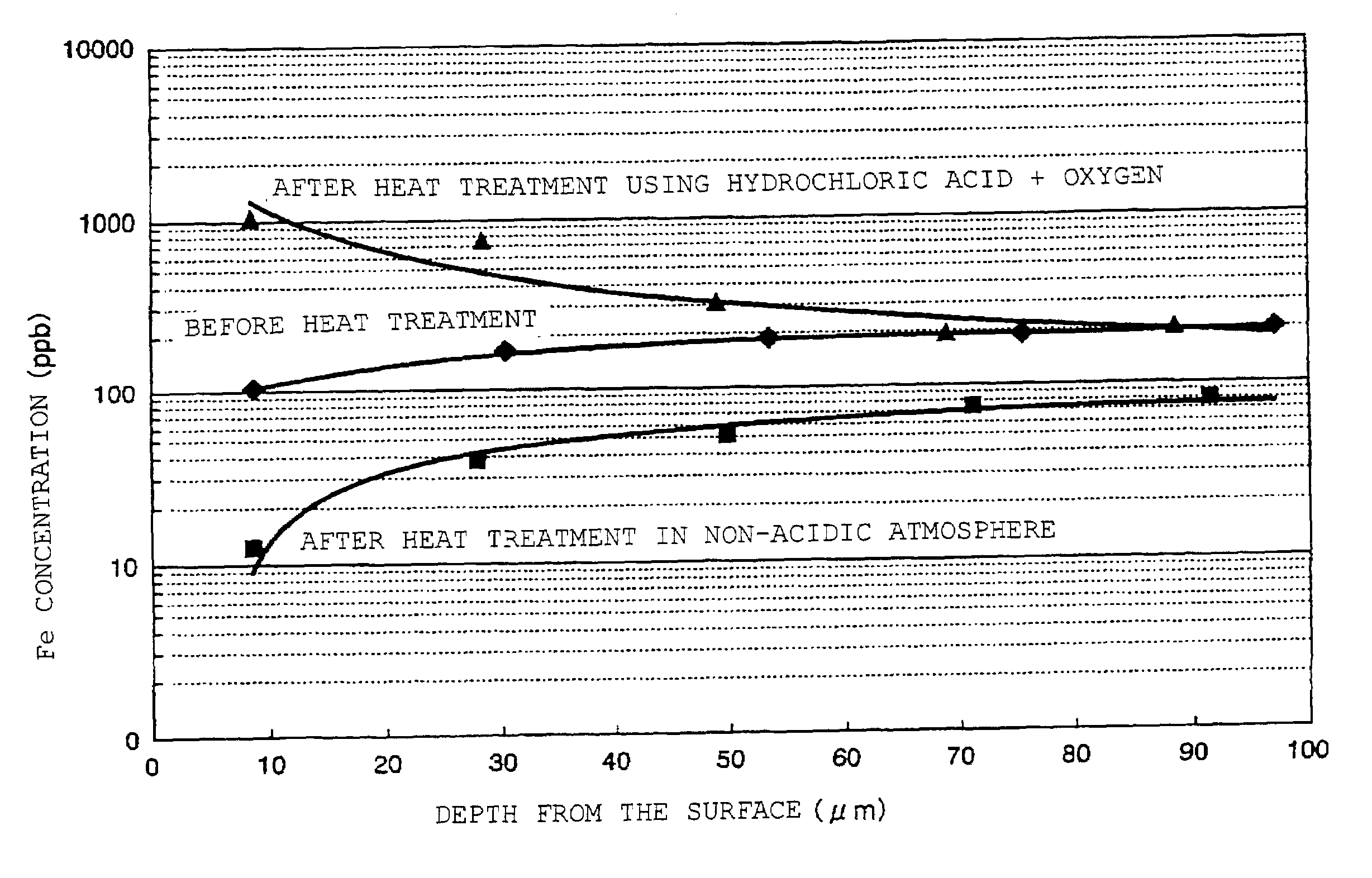
[0039]Also, each concentration of Fe, Cu, Cr and Ni was measured by an ICP mass spectrometer. As a result, the concentrations at each depth from the surface were as shown in Table 1.

[0040]Next, the sample of the highly heat-resistant soot remelted synthetic silica glass was heat-treated at 1...


PUM

PropertyMeasurementUnit
temperatureaaaaaaaaaa
viscosityaaaaaaaaaa

Abstract

A silica glass member for semiconductor in which each concentration of Fe, Cu, Cr and Ni is 5 ppb or less and the concentration of an OH group is 30 ppm or less and which has a viscosity of 1013.0 poise or more at 1200° C. is provided as a silica glass member for semiconductor having high heat-resistance and higher purity.

Description

BACKGROUND OF THE INVENTION[0001]1. Field of the Invention[0002]The invention relates to a silica glass member for semiconductor such as a furnace core tube, a wafer boat and a heat insulating mould used for the production of a semiconductor and a production method thereof.[0003]2. Description of the Related Art[0004]Conventionally, as silica glass members for semiconductor of this kind, those comprising electrically melted quartz glass which is produced by melting a natural crystal in an electric furnace and then solidifying, those comprising an OH group (hydroxyl group)-containing soot remelted synthetic silica glass produced by hydrolyzing a silicon compound such as silicon tetrachloride in an oxyhydrogen flame and then melting or those comprising highly heat-resistant soot remelted synthetic silica produced by processing a porous body of a synthetic silica powder obtained by hydrolyzing a silicon compound such as silicon tetrachloride in an oxyhydrogen flame and deposited on a s...

Claims


Application Information

Patent Timeline
Patent Type & Authority Patents(United States)
IPC IPC(8): C03B20/00C03B8/04C03C3/06C03C15/00C30B35/00
CPCC03C3/06C03C15/00C30B35/00C03C2203/52C03C2201/02
Inventor EZAKI, MASANOBUPAN, LIAN-SHENGTANIIKE, SEIJI
Owner COVALENT MATERIALS CORP
Learn More