
Function reconfigurable semiconductor device and integrated circuit configuring the semiconductor device

a semiconductor device and integrated circuit technology, applied in pulse manipulation, pulse technique, instruments, etc., can solve the problems of difficult reconfiguration, large circuit scale, difficult reconfiguration of logic functions, etc., and achieve the effect of reducing the area used for implementing devices and circuits, logic capability, and reconfiguring function capabilities

Inactive Publication Date: 2006-07-11
NIPPON TELEGRAPH & TELEPHONE CORP
View PDF14 Cites 23 Cited by
  • Summary
  • Abstract
  • Description
  • Claims
  • Application Information

AI Technical Summary

Benefits of technology

The present invention provides a semiconductor device and an integrated circuit that decrease or do not use a memory element or a memory circuit for storing function configuration data in the programmable hardware, thus decreasing the area used for implementing the device and increasing its performance. Additionally, the invention provides a method for realizing a function quickly by using a neuron MOS circuit. The invention also provides a function reconfigurable semiconductor device and integrated circuit that can easily change the function it realizes, and a method for realizing a function using neuron MOS transistors. The invention also provides a method for realizing a function using a circuit that stores function configuration data for determining the function.

Problems solved by technology

Thus, the scale of the circuit becomes large.
However, it is difficult to reconfigure a logic function after a logic function is configured.
However, there is a problem in that reconfiguration is difficult after a logic is configured once.
Thus, it is difficult to reconfigure a logic function easily and for a short time.
Especially, as for the case of the EPROM, since irradiating ultraviolet is necessary for rewriting the logic function, it is not easy to reconfiguring the logic function.
Thus, it is difficult to perform data writing and data erasing speedily.
When an advanced programmable hardware is desired, wherein the advanced programmable hardware can process multilevel and / or analog signals as well as the two-valued signals, the conventional method lacks flexibility.
As mentioned above, when the SRAM is used for storing the function configuration data, area in the chip becomes large.
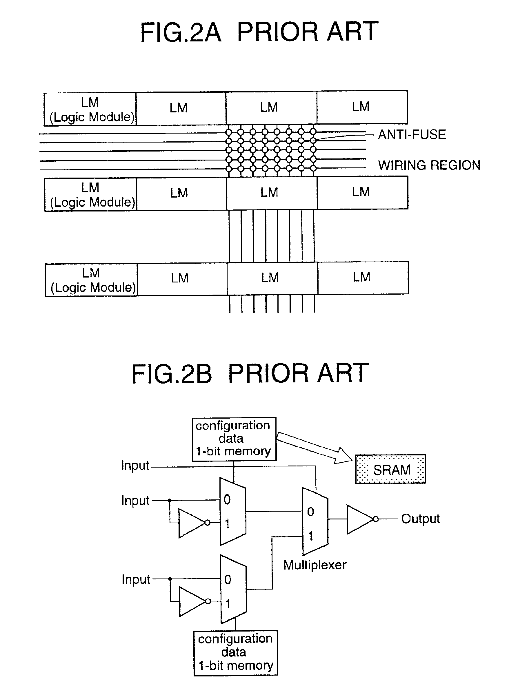
When the anti-fuse is used, reconfiguration is difficult.
As for EPROM and EEPROM, a rewriting specific device becomes necessary so that there is a problem in that reconfiguration is not performed fast.
In addition, it lacks flexibility when advanced programmable hardware is desired.
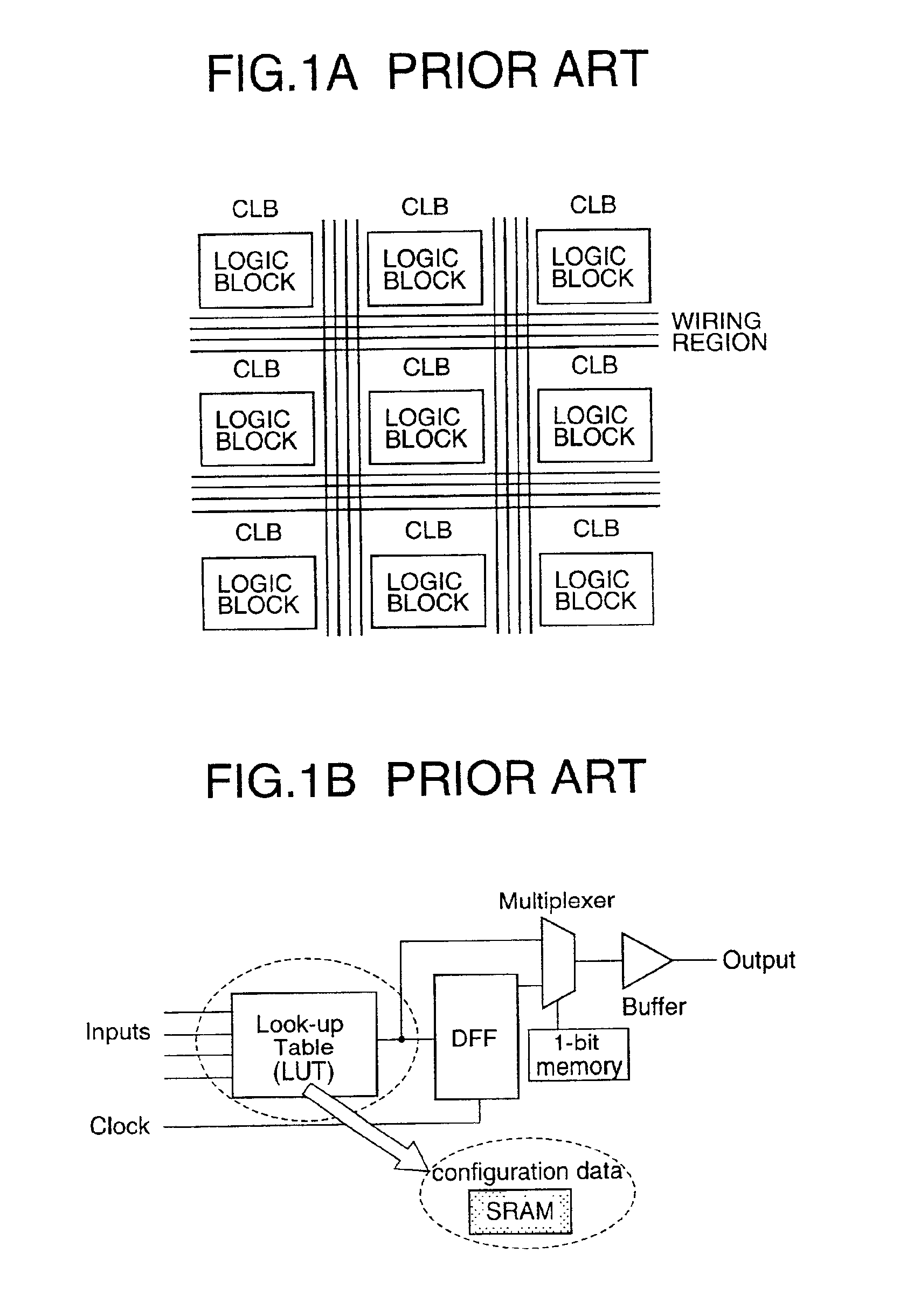
Therefore, there is a problem in that the area cost of the changeable logic part of the LUT type is high.
However, it is difficult for the conventional reconfigurable logic device to realize only special functions having special properties.
Therefore, reconfiguration of the logic function after manufacturing is impossible.
Therefore, this document does not discloses an idea that the neuron MOS circuit holds function or logic configuration data.
This is not very useful.
As mentioned above, there are following problems in the conventional programmable hardware.
As for the multiplexer type and the PLA type, the anti-fuse or memory elements such as EEPROMs and EPROMs are required so that reconfiguring the logic function can not be performed easily and in a short time, wherein it is very difficult for the anti-fuse to reconfigure the logic function due to the principle and the EEPROM requires a specific device for data writing and deleting.
However, there is a problem in that a large area is required in the LSI.

Method used


Image

  • Function reconfigurable semiconductor device and integrated circuit configuring the semiconductor device
  • Function reconfigurable semiconductor device and integrated circuit configuring the semiconductor device
  • Function reconfigurable semiconductor device and integrated circuit configuring the semiconductor device

Examples


embodiment 1-1

[0325](Embodiment 1-1)

[0326]FIG. 7 shows a function reconfigurable semiconductor device according to an embodiment of the present invention. The function reconfigurable semiconductor device includes function cells 101 arranged like an array, wherein the function cells 101 are connected by wiring which can change a connection state. In addition, the function reconfigurable semiconductor device includes a centralized nonvolatile memory circuit 102 which is connected to the function cells via a control circuit block 104. Each of the function cells is an integrated circuit which includes after-mentioned threshold elements. Further, the function reconfigurable semiconductor device has an input circuit block 105 and an output circuit block 106.

[0327]In FIG. 7, input signal lines and output signal lines of the function cell 101 are connected to wiring provided between the function cells via elements or switches 103 which switch connection states.

[0328]The centralized nonvolatile memory cir...

embodiment 1-2

[0368](Embodiment 1-2)

[0369]FIG. 18 shows a function reconfigurable semiconductor device wherein nonvolatile memory circuits for storing function data are distributed so that each function cell has the nonvolatile memory circuit according to the embodiment 1-2 of the present invention. That is, instead of providing the nonvolatile memory circuit 102 shown in FIG. 7, the nonvolatile memory circuit 122 is provided to each function cell 121. The nonvolatile memory circuit 122 can be configured by an EEPROM circuit, a flash memory circuit, a memory circuit using a ferroelectric material or MRAM.

embodiment 1-3

[0370](Embodiment 1-3)

[0371]FIG. 19 shows a function reconfigurable semiconductor device wherein nonvolatile memory circuits 132 are distributed and provided in the function cells, and no wiring area exists. The wiring area is not necessary since the function cells are also used as wiring for the routing of interconnections among them.

[0372]A realizing method of the wiring for the structure shown in FIG. 19 will be described with reference to FIG. 8 and FIG. 20. The structures shown in FIG. 20 and FIG. 16 are similar except that switches are added in the structure shown in FIG. 20.

[0373]In the structure shown in FIG. 20, terminals input1[1]˜input1[3] and input1[2]˜input2[4] are configured to connect to the nonvolatile memory circuit. As mentioned before, by using the init signal shown in FIG. 8, the input variables input from the terminals input1[1]˜input1[3] are stored. That is, the input status number is fixed as a number. As described in the embodiment 1-1, the output value of th...


PUM


Abstract

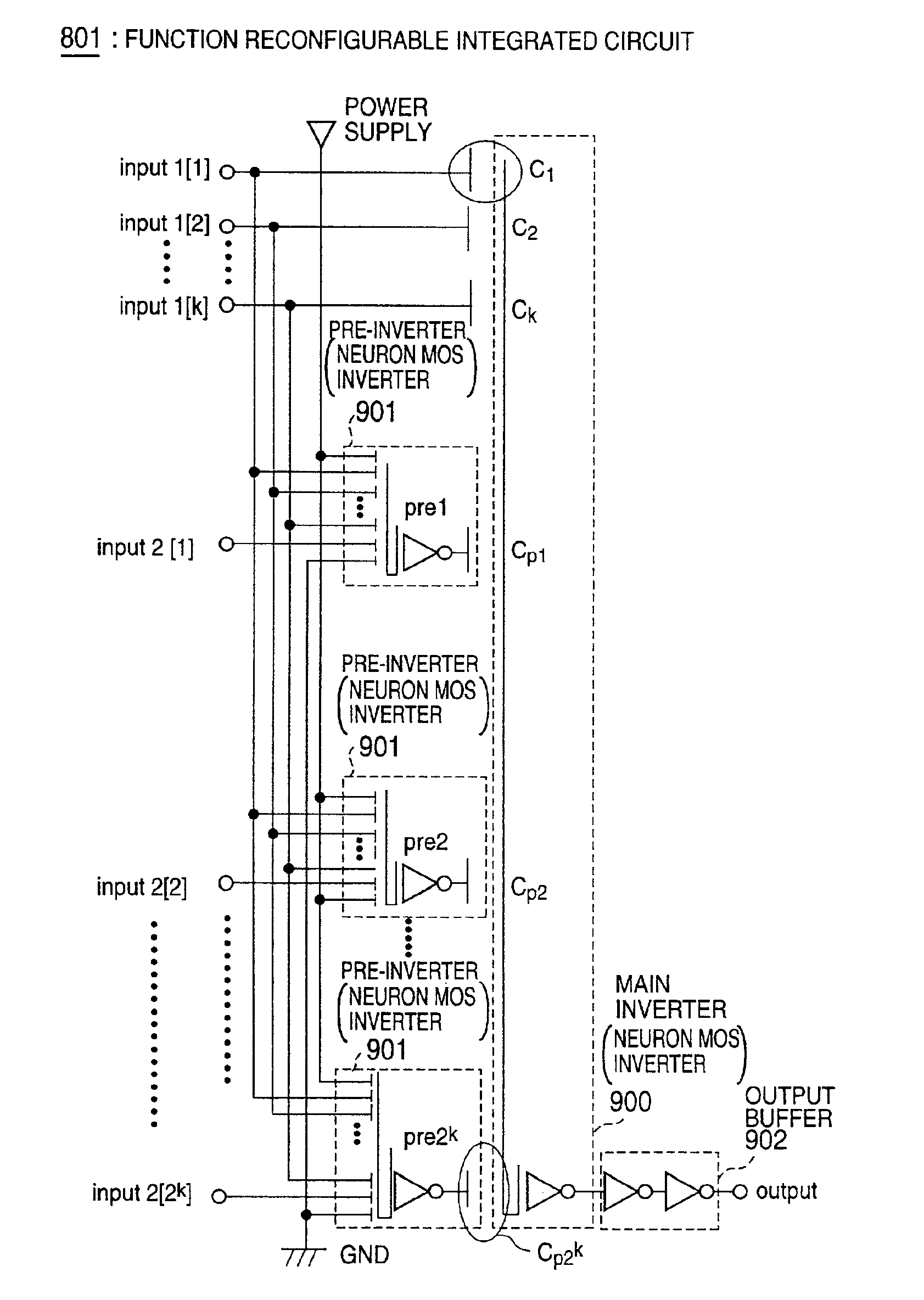
A function reconfigurable semiconductor device is provided. The function reconfigurable semiconductor device includes a plurality of function cells, each of the function cells being a basic unit which realizes a function; each of the function cells including a plurality of threshold elements; each of the threshold elements including means which stores a threshold value; and wherein a function which is realized by the function cell is determined by determining the threshold value in each of the threshold elements. In addition, the semiconductor device includes a nonvolatile memory which stores data for realizing the function in the function cells.

Description

BACKGROUND OF THE INVENTION[0001]1. Field of the Invention[0002]The present invention relates to a semiconductor device and an integrated circuit. More particularly, the present invention relates to the semiconductor device and the integrated circuit which can configure a function in each of them even after they are manufactured. In addition, the present invention relates to a method of storing function configuration data.[0003]Further, the present invention relates to an integrated circuit which can configure any symmetric function in it and has a selector capability.[0004]Further, the present invention relates to a method of designing an integrated circuit which realizes any function and relates to the integrated circuit.[0005]2. Description of the Related Art[0006]A reconfigurable logic device, typified by FPGA (Field Programmable Gate Array) or PLD (Programmable Logic Device) becomes widely used for various purposes in addition that the scale of it becomes larger.[0007]When the ...

Claims


Application Information

Patent Timeline
Patent Type & Authority Patents(United States)
IPC IPC(8): G11C16/04G06F15/78G06N3/063
CPCG06F15/7867G06N3/0635G11C27/005H03K5/133H03K19/08H03K19/17736H03K19/17748H03K19/1776H03K19/1778H03K19/0813H03K2005/00156G06N3/065
Inventor AOYAMA, KAZUOSAWADA, HIROSHINAGOYA, AKIRANAKAJIMA, KAZUOSHIBATA, TADASHI
Owner NIPPON TELEGRAPH & TELEPHONE CORP
Learn More