
Back-drive circuit protection for I/O cells using CMOS process

a back-drive circuit and i/o cell technology, applied in the direction of pulse technique, oscillation generator, reliability increasing modifications, etc., can solve the problems of sub-micron dual gate device problems, i/o cell heating and possible latch-up, oxide breakdown, etc., to enhance the tolerance of the drive circuit

Inactive Publication Date: 2006-07-04
NAT SEMICON CORP
View PDF2 Cites 8 Cited by
  • Summary
  • Abstract
  • Description
  • Claims
  • Application Information

AI Technical Summary

Benefits of technology

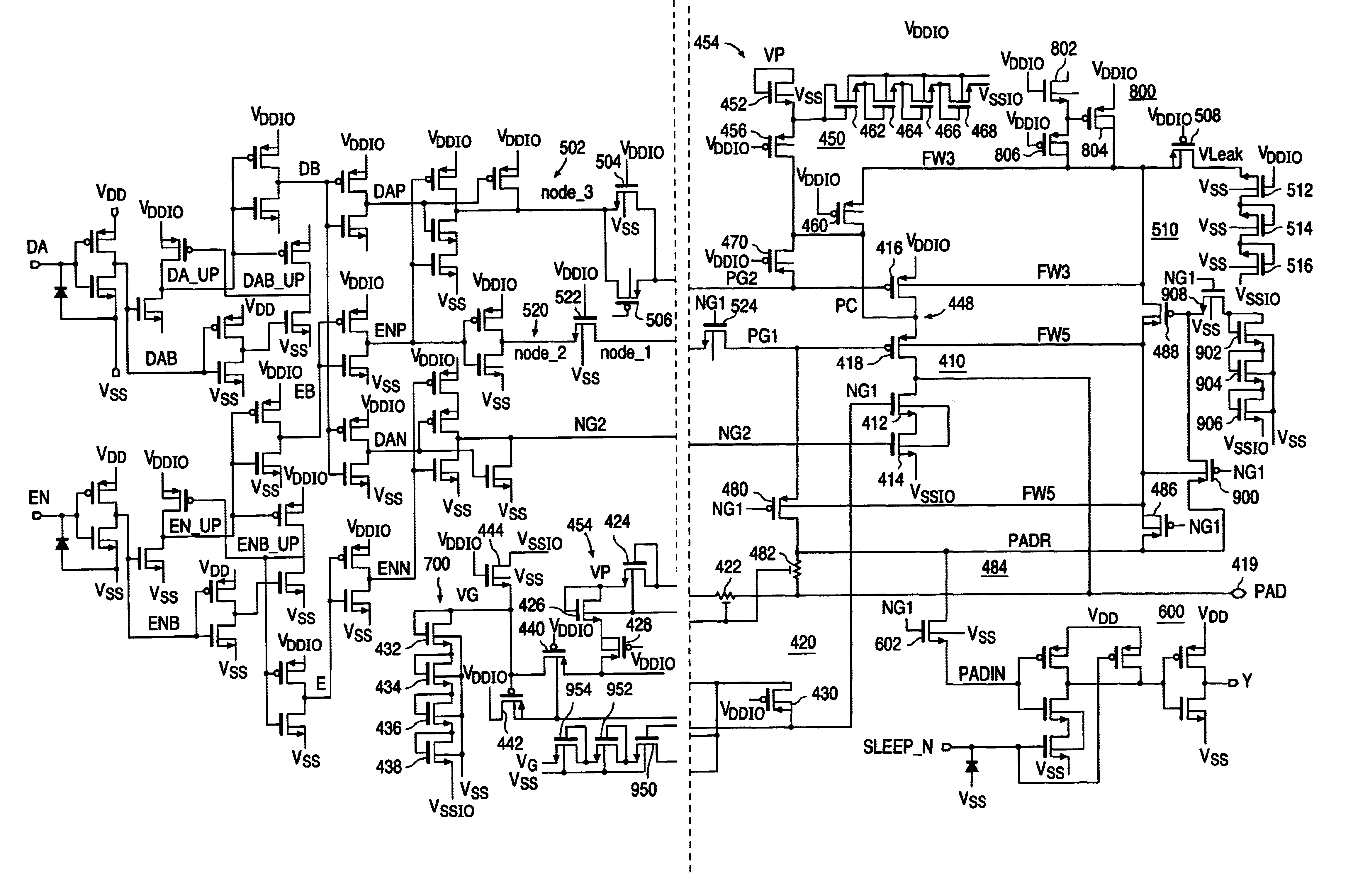
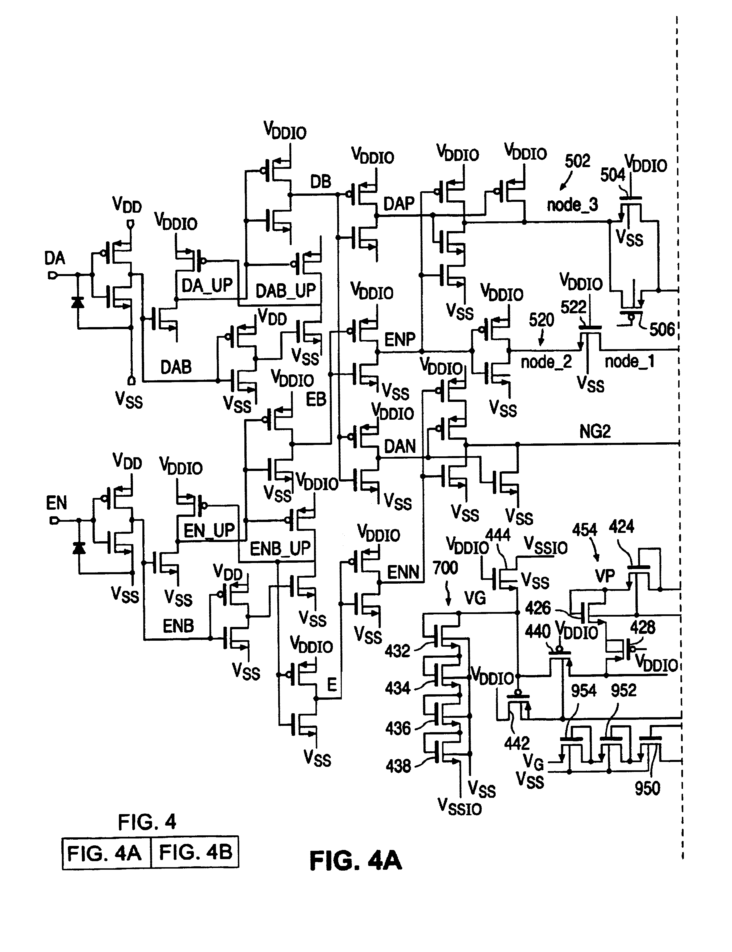
[0015]Further, according to the invention, there is provided a method of enhancing the tolerance of a drive circuit during stress mode, comprising providing a cascoded circuit of a first PMOS transistor connected to a pad, a second PMOS transistor, and first and second NMOS transistors, charging the gates of the PMOS transistors to avoid gate oxide breakdown, clamping the node between the PMOS transistors to avoid junction breakdown of the second PMOS transistor, switching off both PMOS transistors during stress mode, and providing a current path to ground for leakage current flowing through the reverse biased parasitic diode of the first PMOS transistor.

Problems solved by technology

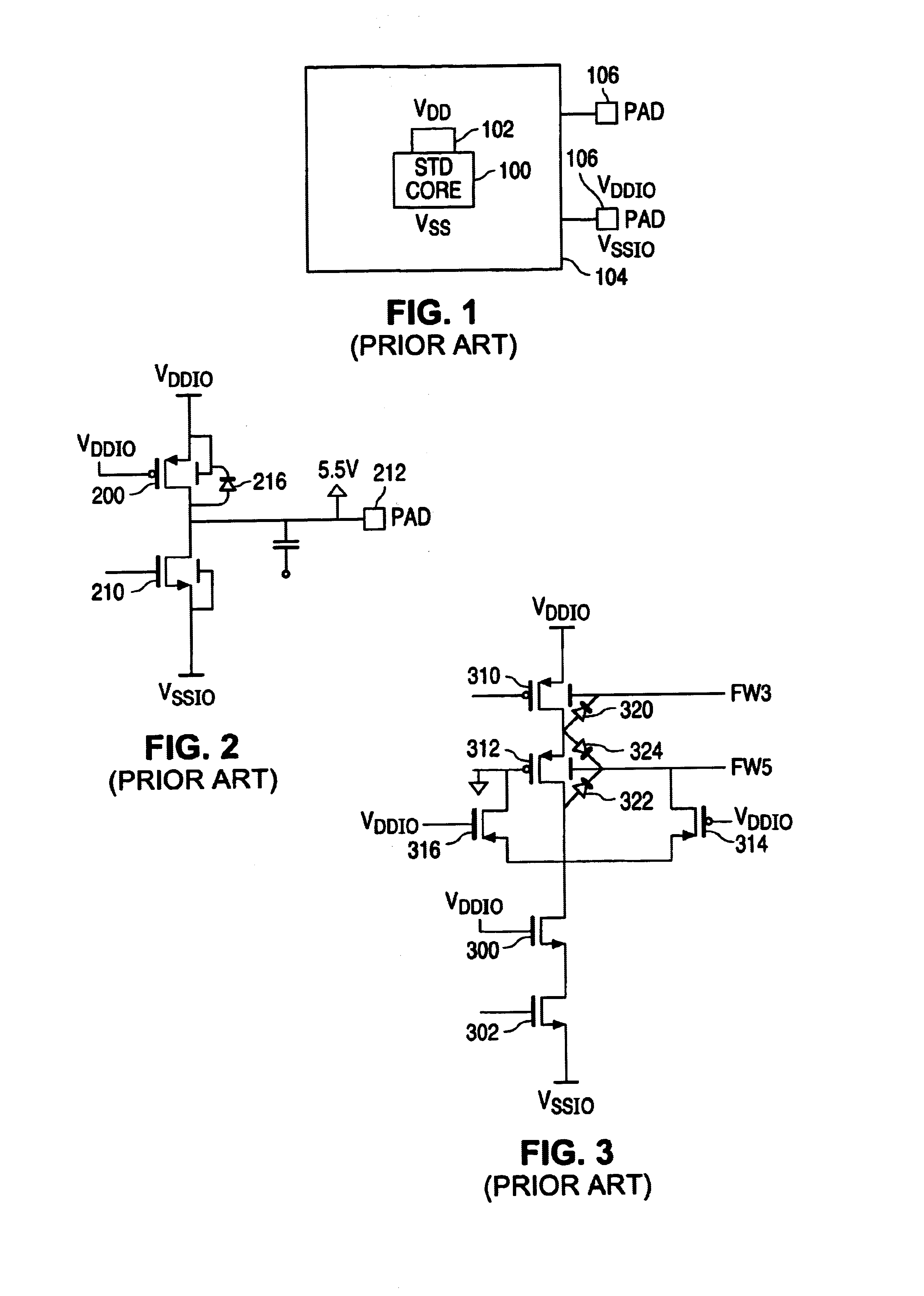
However, under stress mode, sub-micron dual gate devices tend to experience problems such as oxide breakdown, drain-source junction breakdown, current flow to VDDIO, and well charging due to the parasitic internal diode structure of CMOS devices.
This results in heating of the cell and possible latch-up.

Method used


Image

  • Back-drive circuit protection for I/O cells using CMOS process
  • Back-drive circuit protection for I/O cells using CMOS process
  • Back-drive circuit protection for I/O cells using CMOS process

Examples


Embodiment Construction

[0020]The present invention proposes certain changes and additions to a cascoded driver circuit in order to improve tolerance under stress mode. In particular, the invention seeks to avoid gate oxide breakdown of the PMOS transistors by charging up the gates so that the gate-drain voltage is always less than 3.8 V. It also seeks to avoid current to VDDIO by switching the PMOS transistors off. This is achieved by charging the gates of the transistors to the same voltage as the high voltage node (drain) during stress mode. The invention also seeks to avoid parasitic well charging of the PMOS transistors by charging the wells to the same voltage as their respective high voltage nodes (drains). The invention also seeks to avoid drain-source junction breakdown of the upper PMOS transistor by reducing the potential difference across the transistor to less than 3.8 V. This is achieved by charging the drain of the upper PMOS transistor to approximately 3.3 V. The invention further seeks to ...


PUM


Abstract

In a high tolerance I / O interface with over-voltage protection beyond 5 V, a cascoded driver with PMOS pull-up and NMOS pull-down transistors, connected to a pad, is provided. Circuitry is included to maintain the floating well voltages of the PMOS pull-up driver transistors at substantially the same voltages as their respective drains, and their gate voltages at substantially the same voltages as their respective drains, under back-drive and 5 V tolerant mode. Circuitry is also provided to increase the gate voltage of one of a cascoded pair of NMOS pull-down driver transistors, so that the drain-source junction voltage and gate oxide voltage of the transistor will be less than the breakdown voltage under back-drive and 5 V tolerant mode.

Description

FILED OF THE INVENTION[0001]The invention relates to a method and system for providing back-drive circuit protection for I / O cells in a CMOS integrated circuit device.BACKGROUND OF THE INVENTION[0002]A typical integrated circuit device (IC) includes a core region 100, as illustrated in FIG. 1, and one or more functional elements or packages such as analog support / conversion circuitry 102. These are connected through an I / O interface 104 to pads 106 that allow the IC to be connected externally to other devices. The voltage levels vary for different portions of the IC, thus requiring special consideration to avoid exposing the various portions of the IC to excessive voltage levels. For instance, the core, I / O interface, and external circuitry to which the pads of the IC connect, typically will each support different voltages. Even within a typical CMOS core, voltages vary depending on the process used. For example, a 0.25 μm process supports voltage levels of the order of 2.5 V±10%; a...

Claims


Application Information

Patent Timeline
Patent Type & Authority Patents(United States)
IPC IPC(8): H03K3/00
CPCH03K19/00315H01L27/0266
Inventor KIANI, KHUSROW
Owner NAT SEMICON CORP
Learn More