Distributed feedback semiconductor laser for outputting beam of single wavelength

a semiconductor laser and single wavelength technology, applied in the direction of laser details, laser optical resonator construction, optical resonator shape and construction, etc., can solve the problems of low product yield in manufacture, low probability of dfb semiconductor laser oscillation at a single wavelength, and inability to provide accurate control of phase shift amount, etc., to achieve high accuracy, improve output beam wavelength stability, and improve product yield in manufacture

Inactive Publication Date: 2006-06-20
ANRITSU CORP
View PDF11 Cites 3 Cited by
  • Summary
  • Abstract
  • Description
  • Claims
  • Application Information

AI Technical Summary

Benefits of technology

[0043]The present invention has been made under the above-described circumstances, and it is therefore an object of the present invention to provide a DFB semiconductor laser in which output beam wavelength can be set to a desired wavelength at a high accuracy, output beam wavelength stability can be improved, and yield in the manufacture can be improved.

Problems solved by technology

However, the DFB semiconductor laser having the structure shown in FIG. 22 still has the following problems yet to be solved.
As a result, it is impossible to provide accurate control on the amount of the phase shift of the beam that travels on the connecting waveguide 7, and there is a problem that the manufactured DFB semiconductor laser has a low probability for oscillation at a single wavelength, which means that product yield is low in the manufacture.
First, if the length L of the connecting waveguide cannot be selected freely, this restriction affects the overall size and shape of the DFB semiconductor laser and accordingly, the freedom of the device design is limited.
Second, if the length L of the connecting waveguide is short, intensity of the beam outputted by the DFB semiconductor laser is low.
Furthermore, since spatial hole burning is induced, degradation of intensity of the outputted beam or beam spectrum width can often be induced.
To the contrary, if the length L of the connecting waveguide is long, the overall size of the DFB semiconductor laser is increased, and the number of devices manufactured per wafer is decreased, so that the manufacturing cost of the device is increased.
As a result there is a problem that it is difficult to achieve “single-mode oscillation” described above.

Method used


Image

  • Distributed feedback semiconductor laser for outputting beam of single wavelength
  • Distributed feedback semiconductor laser for outputting beam of single wavelength
  • Distributed feedback semiconductor laser for outputting beam of single wavelength

Examples


first embodiment

(First Embodiment)

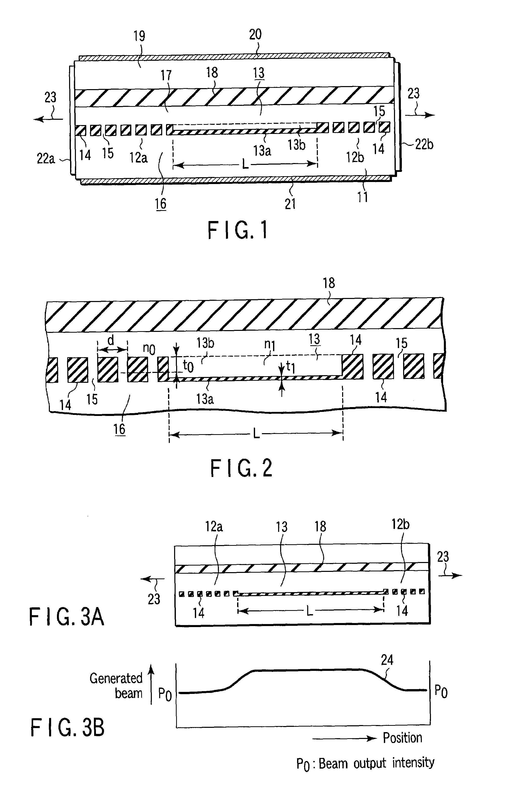
[0160]FIG. 1 is a schematic sectional view for explaining a general configuration of a DFB semiconductor laser according to a first embodiment of the present invention.

[0161]As shown in FIG. 1, the DFB semiconductor laser according to the first embodiment of the present invention comprises a semiconductor substrate 11 of n-type InP, and a first diffraction grating layer 12a of n-type InGaAsP, a connecting layer 13, and a second diffraction grating layer 12b of n-type InGaAsP are formed on an upper surface of the semiconductor substrate 11.

[0162]Each of the first and second diffraction grating layers 12a, 12b includes a plurality of bars 14 and a plurality of slits 15 existing between the bars.

[0163]In this case, all the bars 14 and all the slits 15 included in the first and second diffraction grating layers 12a, 12b configure a virtual diffraction grating 16 that has a constant grating pitch (pitch) and a continuous phase.

[0164]A refractive index of the bars 14 whi...

second embodiment

(Second Embodiment)

[0187]FIG. 5 is a schematic sectional view for explaining a general configuration of a DFB semiconductor laser according to a second embodiment of the present invention.

[0188]In FIG. 5, components identical with those in the DFB semiconductor laser according to the first embodiment shown in FIG. 1 are given the same reference codes and their description will not be duplicated here.

[0189]As shown in FIG. 5, the DFB semiconductor laser according to the second embodiment of the present invention comprises a semiconductor substrate 11 of n-type InP, which has an upper surface formed with an active layer 18 including a lower SCH layer, a MQW layer, and an upper SCH layer, each made of an appropriate combination of InGaAsP.

[0190]A buffer layer 17 made of the same material as a cladding layer 19 is formed on an upper surface of the active layer 18.

[0191]A first diffraction grating layer 12a of p-type InGaAsP, a connecting layer 13, and a second diffraction grating layer ...

third embodiment

(Third Embodiment)

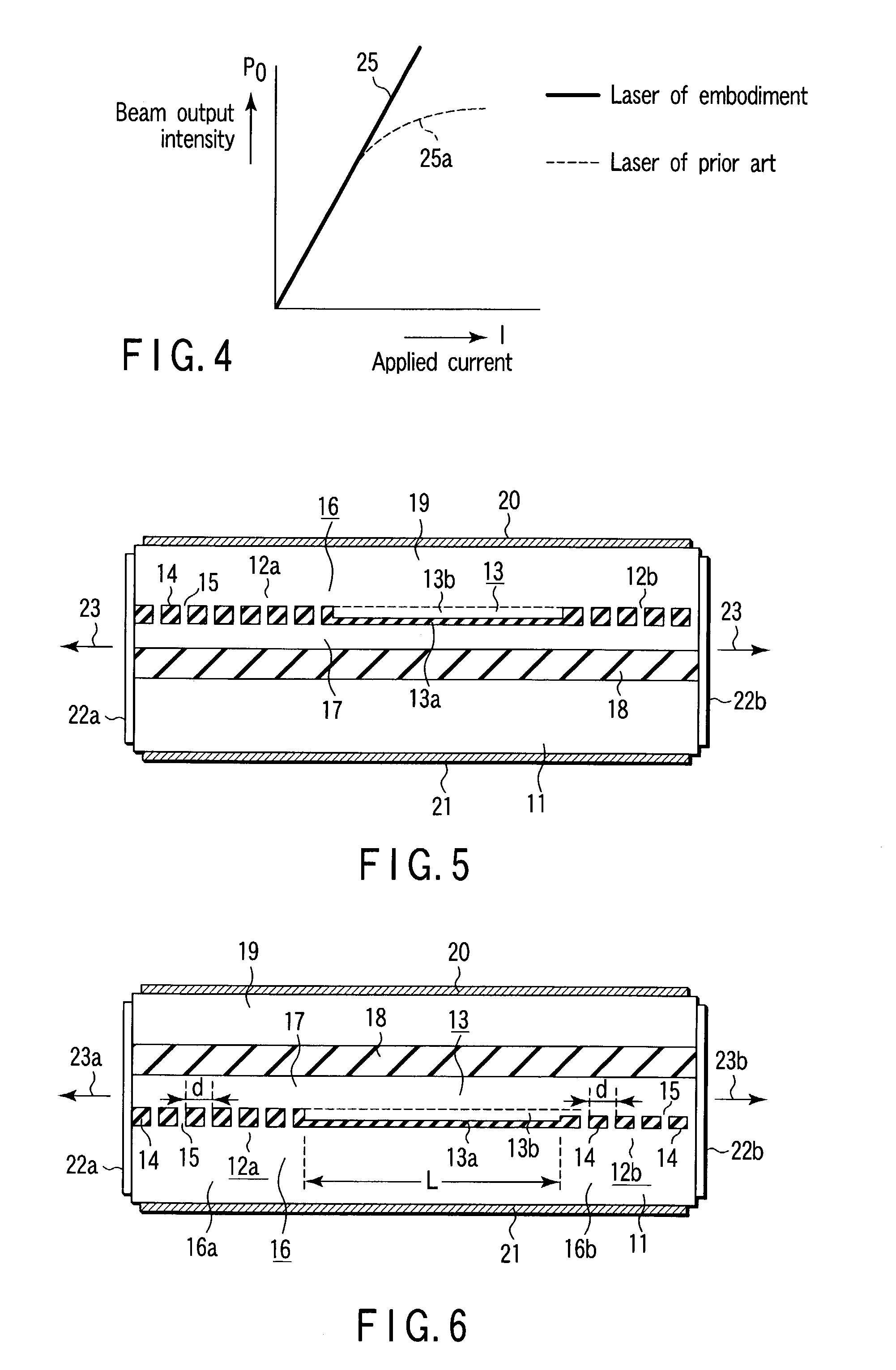
[0205]FIG. 6 is a schematic sectional view for explaining a general configuration of a DFB semiconductor laser according to a third embodiment of the present invention.

[0206]In FIG. 6, components identical with those in the DFB semiconductor laser according to the first embodiment shown in FIG. 1 are given the same reference codes and their description will not be duplicated here.

[0207]As shown in FIG. 6, in the DFB semiconductor laser according to the third embodiment of the present invention, a coupling efficiency κ1 in a diffraction grating 16a of a first diffraction grating layer 12a and a coupling efficiency κ2 in a diffraction grating 16b of a second diffraction grating layer 12b is set to values different from each other.

[0208]Further, in the DFB semiconductor laser according to the third embodiment of the present invention, a volume ratio v1 per grating pitch d in the diffraction grating 16a of the first diffraction grating layer 12a, which is a ratio betwe...


PUM


Abstract

First and second diffraction grating layers are provided above a semiconductor substrate, and are spaced from each other in an output direction of a beam with a flat connecting layer sandwiched therebetween. An active layer is disposed above or below the first and second diffraction grating layers and the connecting layer. A cladding layer is disposed above the active layer or above the first and second diffraction grating layers and the connecting layer. A diffraction grating including the first and second diffraction grating layers has a plurality of slits penetrating from an upper surface to a lower surface that are perpendicular to the output direction of the beam. The connecting layer is formed from two layers grown epitaxially in a direction perpendicular to the output direction of the beam. One of the two layers is formed of the same material as the first and second diffraction grating layers.

Description

CROSS-REFERENCE TO RELATED APPLICATIONS[0001]This application is based upon and claims the benefit of priority from the prior Japanese Patent Applications No. 2002-188530, filed Jun. 27, 2002; and No. 2002-188531, filed Jun. 27, 2002, the entire contents of both of which are incorporated herein by reference.BACKGROUND OF THE INVENTION[0002]1. Field of the Invention[0003]The present invention relates to a distributed feedback semiconductor laser, and more specifically to a distributed feedback semiconductor laser which outputs a beam of a single wavelength for such purposes as optical communication and optical measurement.[0004]2. Description of the Related Art[0005]As shown in FIG. 21A, a conventional semiconductor laser which outputs a beam for use in optical communication and optical measurement comprises, for example, a semiconductor substrate 1, on which an active layer 2 and a cladding layer 3 are grown epitaxially.[0006]In such a semiconductor laser, a beam 4 is outputted from...

Claims


Application Information

Patent Timeline
Patent Type & Authority Patents(United States)
IPC IPC(8): H01S3/08H01S5/00H01S5/12
CPCH01S5/12H01S5/0654H01S5/1203H01S5/1243H01S5/1231H01S5/124H01S5/1225
Inventor MORIKIKUGAWA, TOMOYUKITAKAHASHI, YOSHIOFUJITA, MOTOAKI
Owner ANRITSU CORP
Why Eureka
Try Eureka