Method of forming electrical interconnects having electromigration-inhibiting segments relative to a critical length

a technology of electromigration inhibition and critical length, which is applied in the direction of resistive material coating, solid-state device coating, metallic material coating process, etc., can solve the problem of not ensuring unable to perform photolithography to align stacked strips, and unable to achieve the dimension control required to fabricate devices with submicron feature size, etc. problem, to achieve the effect of reducing the overall resistance increase caused by the electromig

Inactive Publication Date: 2006-06-20
SAMSUNG ELECTRONICS CO LTD
View PDF14 Cites 25 Cited by
  • Summary
  • Abstract
  • Description
  • Claims
  • Application Information

AI Technical Summary

Benefits of technology

[0017]Such process sequence ensures a very short length, and, consequentially, low resistance of electromigration-inhibiting segments. With the conductive segments being relatively long, the overall resistance increase caused by the electromigration-inhibiting segmentation is very small. The improved electromigration-inhibiting resistance of the resulting electrical conductors is ensured by keeping the length of the electrically conductive segments equal to or less than the predetermined critical length, Lc.
[0018]The method also ensures adequate control of the space between equidistant electrical conductors when this space is required to be less than 1 micron. A plurality of equidistant electrical conductors spaced at less than 1 micron can thereby be accurately formed within one layer of metallization using photolithography and dry etching, and multiple layers of metallization can be fabricated in the same way.

Problems solved by technology

However, EM failure is even more likely to occur at the end of a metal conductor where it is attached to an interlevel contact or via.
The first stripe itself is non-planar, making it difficult to perform photolithography to align the stacked stripe.
Because of non-planarity, the process described by Wei Zhang, et al. does not ensure the dimension control which is required to fabricate devices with submicron feature size.
Particularly, it cannot easily be used to fabricate the conductors in high-performance, state-of-the-art Very Large Integrated Circuits (VLSI).
Also, the structure proposed by Wei Zhang et al., does not provide complete blocking of electromigration, because aluminum can migrate away from the contact in the top conducting layer of Al-1% Si.
On the other hand, even though the gap can somewhat prolong the life of the nearby contact, the gap itself creates a flux divergence and is a likely site for an EM failure.
This method has the same disadvantage as the method proposed by Wei Zhang, et al.

Method used


Image

  • Method of forming electrical interconnects having electromigration-inhibiting segments relative to a critical length
  • Method of forming electrical interconnects having electromigration-inhibiting segments relative to a critical length
  • Method of forming electrical interconnects having electromigration-inhibiting segments relative to a critical length

Examples


Embodiment Construction

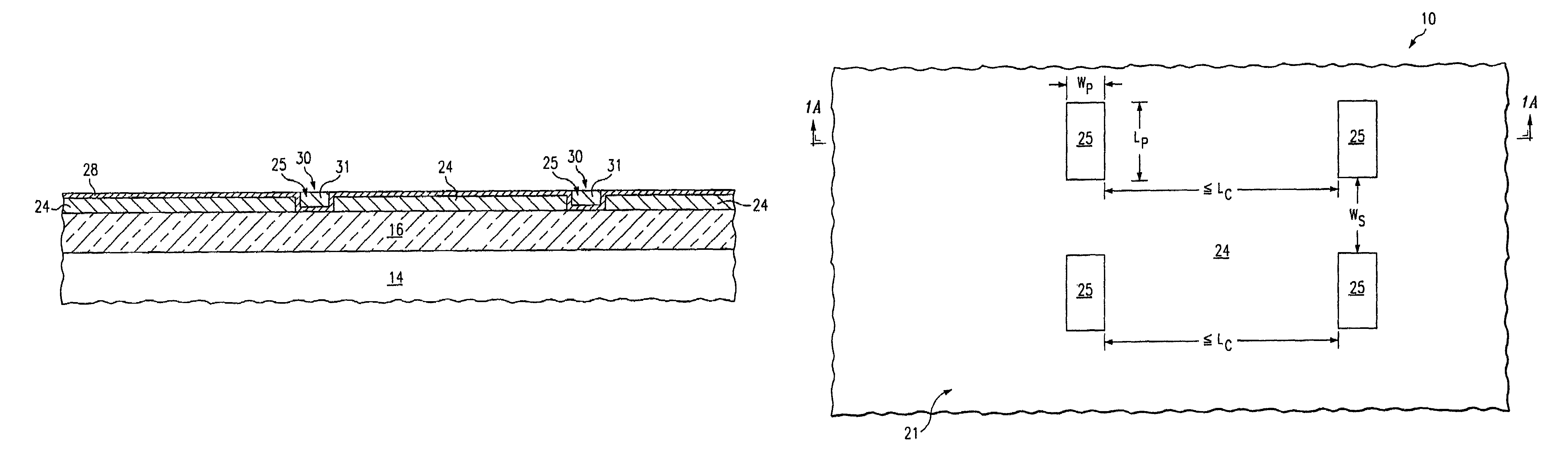
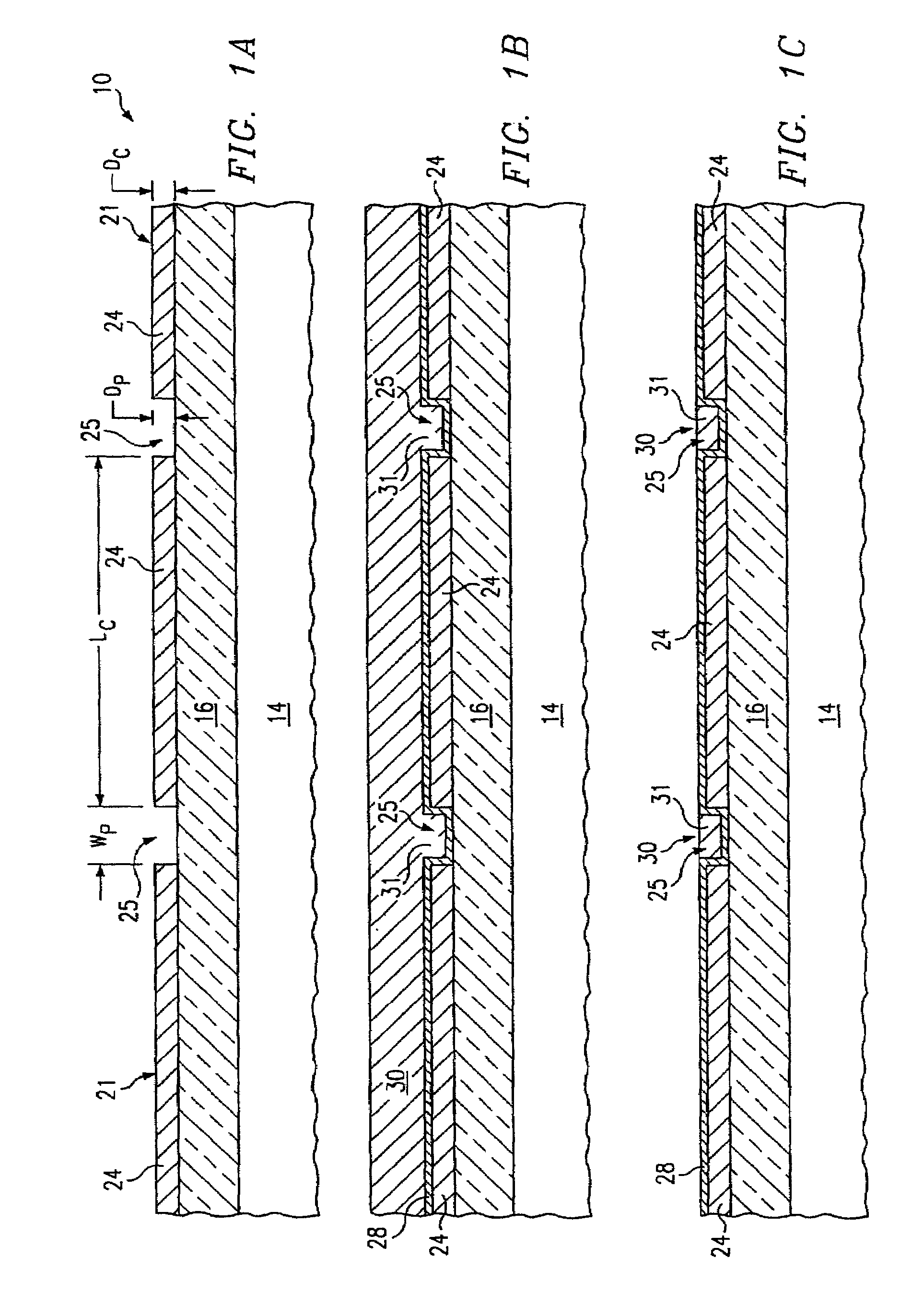
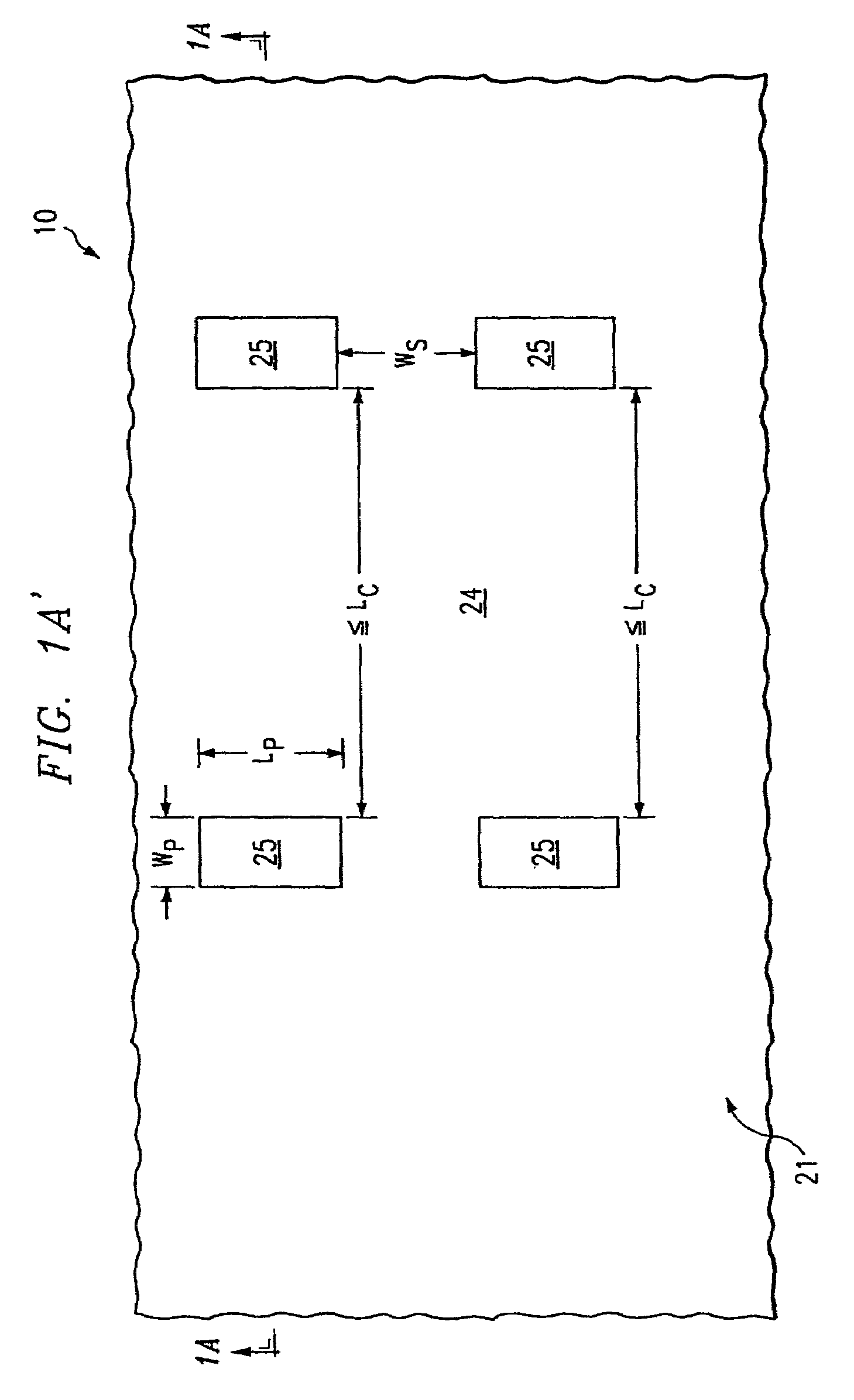
[0034]Referring now to FIG. 1A, a semiconductor structure 10 is shown having a silicon layer 14, and a silicon dioxide layer 16 as shown. A 0.6 micron thick film, or layer 24 of a relatively high electrically conductive material, here an aluminum-copper (Al—Cu) alloy is evaporated over the surface. Other material may be used for film 24, such as Al, Cu, Au, Ag, or their alloys, i.e. the electrically conductive film 24 need not be immune to electromigration. The film 24 alternatively may be a multi-layer structure having one or more additional layers made of conductive materials, such as indicated above, and / or refractory metals or their compounds, such as Ti, W, TiN, TiW, Mo, Ta, or others, which are known to be immune to electromigration at typical operating conditions of silicon integrated circuits. It is noted that the upper surface of film 24 is a planar surface 21.

[0035]Multiple equidistant rows of windows are formed so that they are aligned along the desired paths of conductor...


PUM

PropertyMeasurementUnit
lengthsaaaaaaaaaa
lengthsaaaaaaaaaa
critical length Lcaaaaaaaaaa

Abstract

A method of forming an electrical conductor, comprising forming electrically conductive segments incorporating electromigration-inhibiting plugs. A row of windows is formed in a planar surface and electromigraation-inhibiting material is deposited over the planar surface and into the windows to provide electromigration-inhibiting plugs in the windows. The plugs may be formed by depositing an electromigration-inhibiting liner in the windows and then depositing electrically conductive material to fill the windows. Portions of either or both of the plugs and conductive segments are removed such that the plugs and conductive segments have a coplanar surface. The plugs may be formed in windows in an electrically conductive layer defining the conductive segments. Embodiments of the method may be employed in manufacture of integrated circuit conductor.

Description

[0001]This application is a continuation of application Ser. No. 09 / 735,566 filed Dec. 12, 2000 (U.S. Pat. No. 6,678,951 issued Jan. 20, 2004), which is a divisional application of Application Ser. No. 09 / 316,916 filed May 20, 1999 (Pat. No. 6,245,996 issued Jun. 12, 2001) which is a continuation of application Ser. No. 08 / 722,532 filed Sep. 27, 1996, abandoned.BACKGROUND OF THE INVENTION[0002]This invention relates generally to metallization systems and methods and more particularly to metallization systems and methods suitable for use with very large scale integrated (VLSI) circuits. More particularly, the invention relates to metallization systems having increased electromigration (EM) resistance.[0003]As is known in the art, electromigration (EM) in on-chip electrical interconnects is one of the wearout mechanisms which limit the lifetime of integrated circuits. On-chip interconnects are typically made of highly-conductive, polycrystalline metal films, such as aluminum, copper, ...

Claims


Application Information

Patent Timeline
Patent Type & Authority Patents(United States)
IPC IPC(8): H05K3/10H01L21/441C23C20/02H01L21/3205H01L21/768H01L23/522H01L23/528
CPCH01L21/32051H01L21/76843H01L21/76847H01L21/76852H01L21/76877H01L23/5226H01L23/53223H01L23/528Y10T29/49155Y10S29/016Y10T29/49156Y10T29/49165Y10T29/49128H01L2924/0002
Inventor ATAKOV, EUGENIASHEPELA, ADAMBAIR, LAWRENCECLEMENT, JOHNGIESEKE, BRUCE
Owner SAMSUNG ELECTRONICS CO LTD
Why Eureka
Try Eureka