Method of ion implantation for achieving desired dopant concentration

a technology of ion implantation and dopant concentration, which is applied in the direction of transistors, basic electric elements, electrical equipment, etc., can solve the problems of reducing the operation speed of devices, and achieve the effect of reducing the cost and complexity of forming

Inactive Publication Date: 2006-05-23
BELL SEMICON LLC
View PDF20 Cites 5 Cited by
  • Summary
  • Abstract
  • Description
  • Claims
  • Application Information

AI Technical Summary

Benefits of technology

[0018]The method according to the present invention reduces the cost and complexity of forming MOSFETs with different threshold voltages. A plurality of MOSFETs with a range of threshold voltage values can be formed simultaneously with no additional masking steps.

Problems solved by technology

It is known, however, that there is a counter-effect; as the device operating voltage is reduced the operating speed of the device is also reduced.

Method used


Image

  • Method of ion implantation for achieving desired dopant concentration
  • Method of ion implantation for achieving desired dopant concentration
  • Method of ion implantation for achieving desired dopant concentration

Examples


Embodiment Construction

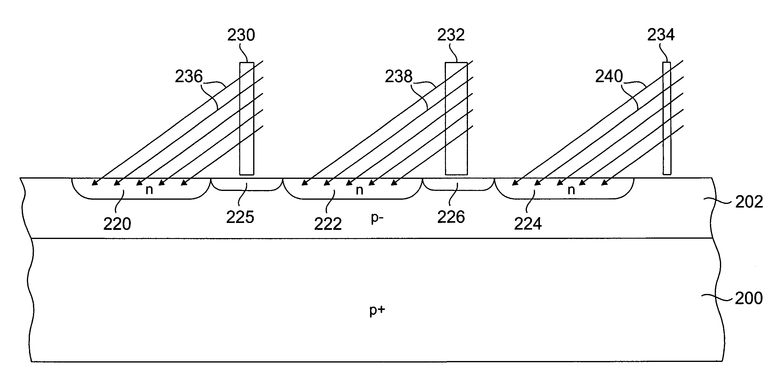
[0037]FIG. 7 is a partial schematic of a prior art CMOS integrated circuit 168 illustrating two pairs of CMOS devices. PMOSFET 170 and NMOSFET 172 form a first CMOS pair; PMOSFET 174 and NMOSFET 176 form a second CMOS pair. Vin1 is the gate driving signal for the PMOSFET 170 and the NMOSFET 172, which creates an output signal (Vout1) at the common drain connection. Vin2 is the gate signal for the CMOS pair PMOSFET 174 and NMOSFET 176, which produces an output signal Vout2. Note further that PMOSFET 170 is responsive to a drain voltage Vdd, and PMOSFET 174 is responsive to a drain voltage Vdd2. The drain voltages Vdd1 and Vdd2 may be produced off-chip or on-chip, although they are illustrated in FIG. 7 as originating from an off-chip voltage source. Because in one embodiment Vdd1 and Vdd2 are not equal, Vout1 is not equal to Vout2. In a typical circuit configuration, both output signals Vout1 and Vout2 drive the next active element in a cascaded circuit chain. For instance, Vout 1 ca...


PUM


Abstract

A method for forming a plurality of MOSFETs wherein each one of the MOSFET has a unique predetermined threshold voltage. A doped well or tub is formed for each MOSFET. A patterned mask is then used to form a material line proximate each semiconductor well, wherein the width of the line is dependent upon the desired threshold voltage for the MOSFET. A tilted ion implantation is performed at an acute angle with respect to the substrate surface such that the ion beam passes through the material line. Thicker lines have a lower transmission coefficient for the ion beam and thus the intensity of the ion beam reaching the adjacent semiconductor well is reduced. By appropriate selection of the line width the dopant density in the well, and thus the final MOSFET threshold voltage, is controllable.

Description

[0001]This application claims the benefit of application Ser. No. 09 / 968,388 filed on Sep. 28, 2001 now abandoned.FIELD OF THE INVENTION[0002]The present invention is directed to semiconductor devices incorporating junctions of varying conductivity types designed to conduct current and methods of making such devices. More specifically, the present invention is directed to metal-oxide field-effect transistors (MOSFETs) having uniquely-determinable threshold voltages and methods for fabricating integrated circuits incorporating such devices.BACKGROUND OF THE INVENTION[0003]As is known to those skilled in the art, most metal-oxide-semiconductor field effect transistors (MOSFETs) are formed in a lateral orientation, with the current flowing parallel to the plane of the substrate or body surface in a channel between a source region and a drain region.[0004]For an enhancement-mode n-channel MOSFET, the substrate is doped p-type and the source and drain regions are diffused or implanted wi...

Claims


Application Information

Patent Timeline
Patent Type & Authority Patents(United States)
IPC IPC(8): H01L21/336H01L21/265H01L27/092H01L21/8234H01L21/8238H01L27/088
CPCH01L21/823807H01L21/26586H01L21/2652H01L21/823892H01L21/265
Inventor LAYMAN, PAUL ARTHURCHAUDHRY, SAMIR
Owner BELL SEMICON LLC
Why Eureka
Try Eureka