Electrooptical devices, electrooptical thin crystal films and methods making same
a thin crystal film and electrooptical technology, applied in the field of electrooptical thin crystal films and methods making same, can solve the problems of low operation speed, short service life, and inability to meet the requirements of the device, and achieve the effect of eliminating the disadvantages inheren
- Summary
- Abstract
- Description
- Claims
- Application Information
AI Technical Summary
Benefits of technology
Problems solved by technology
Method used
Image
Examples
example 1
[0110]This example illustrates the manufacture of an electrooptical anisotropic thin crystal film of a lyotropic liquid crystal based on sulfided indanthrone organic dye.
[0111]The films were prepared from a 9.5% aqueous solution of sulfided indanthrone capable of forming a hexagonal phase at room temperature. This organic dye occurred in the solution in the form of anisometric supramolecular complexes, which formed the basis of a crystal structure of the target film. The initial paste was applied onto a clean silicon or glass substrate by means of casting and spreading. Then the colloid system was treated to reduce the viscosity for the subsequent alignment step. The resulting solution formed a nematic phase or a mixture of nematic and hexagonal phases with a viscosity reduced from 1780 to 250 mPa / s. This preliminary conversion of the colloidal system into a high flow state is a first step before obtaining the high-quality anisotropic thin crystal films of the present invention.
[011...
example 2
[0115]This example illustrates the manufacture of electrooptical devices of the present invention.
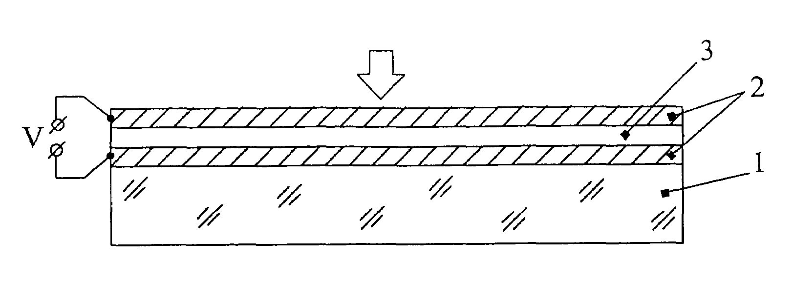
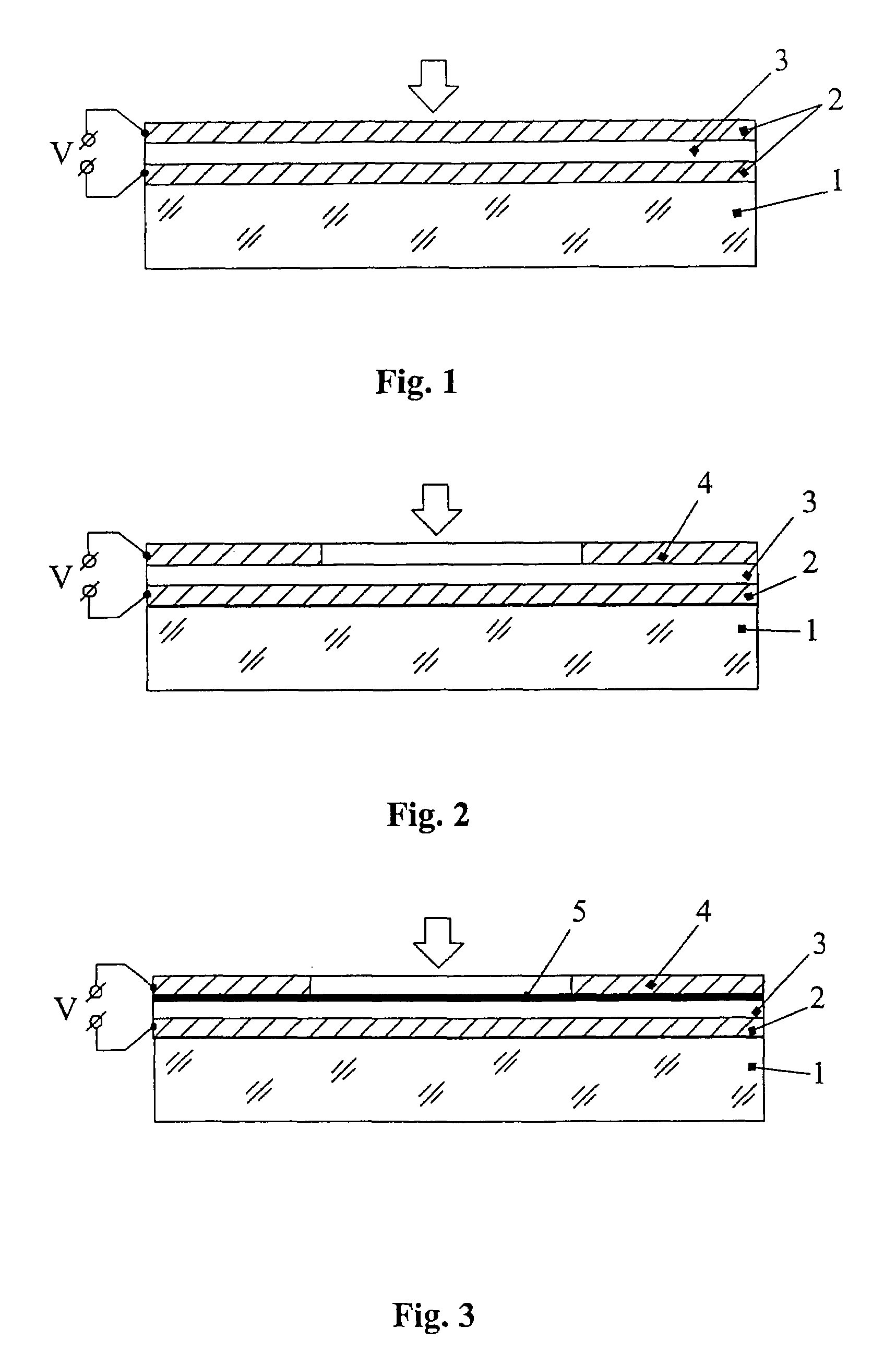
[0116]A layer of SnO2 with a thickness of 0.5 micron was formed by a conventional method. Above this film, an electrooptical anisotropic thin crystal film was formed according to the above described method, which was filled by a protective acetate film with a thickness of 10–20 nm. Then aluminum strips of four millimeter wide were deposited in vacuum onto the acetate film surface. Finally, the electrodes were attached and connected to a source of dc and / or ac control voltage.
example 3
[0117]This example illustrates the manufacture of an electrooptical device based on a D-shaped optical fiber
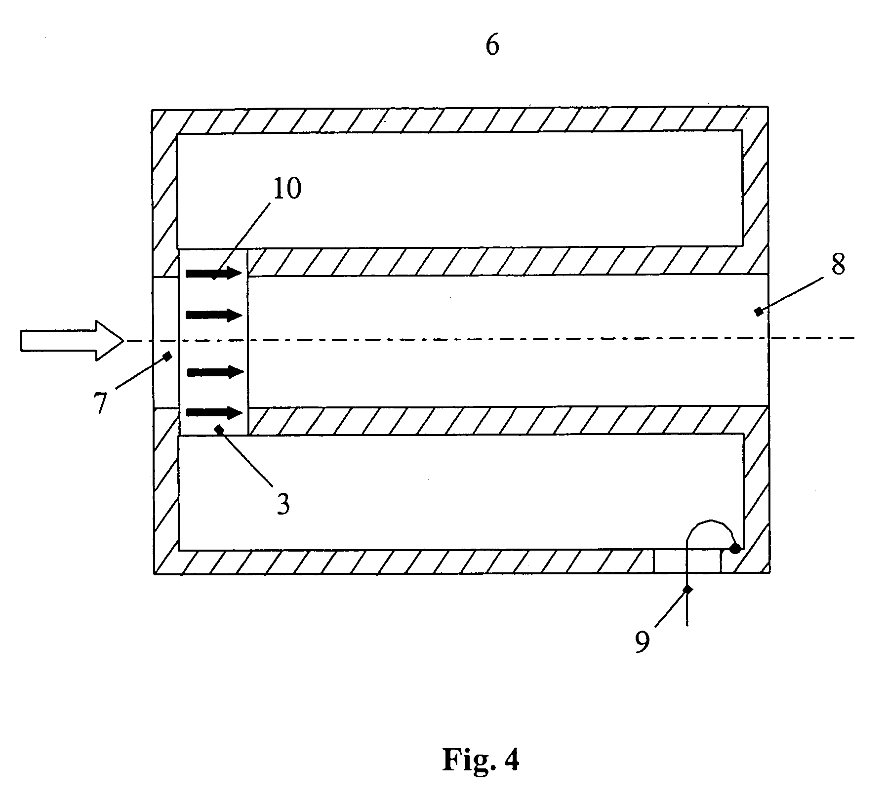
[0118]A metal film was deposited on the flat surface of a D-shaped optical fiber. Then a gap of about five to ten micron wide was formed by a laser beam to divide the metal layer into two electrodes. Finally, an electrooptical anisotropic thin crystal film was formed above this multilayer structure according to the above described method.
[0119]Of advantages, the electrooptical devices of the present invention is capable of controlling radiation in the visible and near IR range. The electrooptical devices of the invention comprises layers of materials with variable refractive indices and / or absorption coefficients dependent on the strength of an applied electric field and / or the electric field component of visible or IR radiation. The electrooptical materials used in the present invention possess a number of useful properties including linear variation of the refractive index d...
PUM
| Property | Measurement | Unit |
|---|---|---|
| angle | aaaaa | aaaaa |
| angle | aaaaa | aaaaa |
| thickness | aaaaa | aaaaa |
Abstract
Description
Claims
Application Information
 - R&D
- Intellectual Property
- Life Sciences
- Materials
- Tech Scout
- Unparalleled Data Quality
- Higher Quality Content
- 60% Fewer Hallucinations
Browse by: Latest US Patents, China's latest patents, Technical Efficacy Thesaurus, Application Domain, Technology Topic, Popular Technical Reports.
© 2025 PatSnap. All rights reserved.Legal|Privacy policy|Modern Slavery Act Transparency Statement|Sitemap|About US| Contact US: help@patsnap.com


