
Apparatus and method for reading out defect information items from an integrated chip

a technology of defect information and integrated chips, which is applied in the direction of digital storage, instruments, measurement devices, etc., can solve the problems of large chip area, large amount of internal logic circuits, and virtually unavoidable defects relating to individual memory cells or groups of memory cells

Inactive Publication Date: 2006-05-02
POLARIS INNOVATIONS LTD
View PDF6 Cites 14 Cited by
  • Summary
  • Abstract
  • Description
  • Claims
  • Application Information

AI Technical Summary

Benefits of technology

[0015]The method according to one embodiment of the invention makes it possible firstly to buffer-store the defect information items of memory cells along a bit line, which are determined by the successive activation and deactivation of word lines of a word line group, in order subsequently to be able to output a compressed defect information item to the test system. The compressed defect information item then makes it possible to ascertain more simply in the test system, i.e., with simplified calculation in the test system, whether defects on word lines of a word line group can be replaced by a common word line group.
[0019]In this respect, it may be provided, for example, that the integrated memory circuit has a plurality of memory arrays each comprising memory cells arranged on word lines and bit lines. The memory cells of the word line group in the plurality of memory arrays may be in this case read substantially simultaneously. The generation of the second defect information items is carried out for each of the plurality of memory arrays. The second defect information items may be buffer-stored and then output successively after the end of the read-out of the memory cells of the word line group along the bit line. The memory arrays are usually called memory banks and are essentially addressable by the address data independently of one another and simultaneously. As a result, it is possible to carry out the method according to one embodiment the invention simultaneously in the plurality of memory arrays, so that, as a result, second defect information items are made available for the memory cells along a bit line and on a word line group for each of the memory arrays. Thus, in the case of four memory banks as commonly provided in a memory chip, after a successive read-out of the memory cells on the word lines of a word line group in each memory bank, four second defect information items are available, which can be subsequently output to the test system at the same time as the testing of further memory cells. This makes it possible for the test time not to be increased even though memory cells along a bit line are tested successively, which usually takes place so slowly that a direct transmission of the first defect information items thereby determined would considerably lengthen the test time.
[0020]Another embodiment provides that a bit line group having a plurality of bit lines may be replaced by a redundant bit line group in order to replace defective memory cells. In the successive read-out of the memory cells on the word lines of the word line group and along the bit line group, third defect information items are generated depending on the result of the comparison for each of the corresponding memory cells, said third defect information items indicating whether a defect has occurred in one of the memory cells of the bit line group. The first defect information items are generated from the third defect information items by means of a compression, so that the first defect information item indicates a defect if one of the third defect information items indicates a defect. In this way, it is possible to achieve a further compression of the defect information items, only a defect information item obtained for a memory segment defined by the address of a word line group and the address of a bit line group being provided in order to be transmitted to the test system. In the case of word line groups having four word lines and bit line groups having four bit lines, a defect information item having the size of one bit can thus be generated for a memory segment comprising 16 memory cells, so that it is possible to achieve a compression of the defect information items by the factor 16.
[0022]In this way, it is possible to provide an integrated memory circuit which makes it possible to successively test memory cells along a bit line and to provide a compressed defect information item which indicates whether the memory cells on a word line group or along a bit line are defective. The compression effected in the integrated memory circuit makes it possible to utilize the time of reading the memory cells on the word line group and along the bit line to communicate defect information items which have already been determined or other information items to the test system via the tester channel. Consequently, time is saved in the test system calculations since a determination as to whether a defect has occurred in a memory area defined by a word line group and a bit line and whether to replace the corresponding word line group by a redundant word line group in the case of a defect can be obviated or considerably simplified.

Problems solved by technology

During the fabrication of DRAM memory chips, the occurrence of defects relating to individual memory cells or groups of memory cells is virtually unavoidable.
In this case, defect information items are often already compressed internally in the memory chip such that no information required for the repair of the defective memory cells is lost.
These internal logic circuits require a considerable chip area and are typically dispensed with for cost reasons.
This is very slow, however, since, each time an address is read out, the previous word line has to be deactivated and a new word line activated, which gives rise to a read-out pause.

Method used


Image

  • Apparatus and method for reading out defect information items from an integrated chip
  • Apparatus and method for reading out defect information items from an integrated chip

Examples


Embodiment Construction

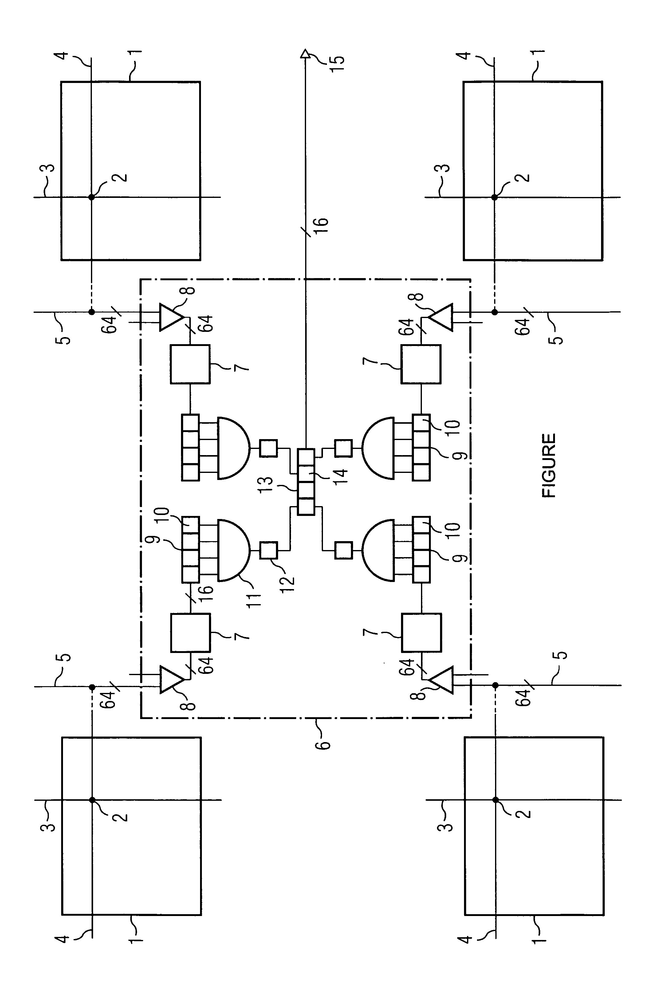
[0027]The FIGURE schematically illustrates an integrated memory circuit having four memory banks 1. In the memory banks 1, memory cells 2 are in each case arranged on word lines 3 and bit lines 4. For the sake of clarity, the FIGURE illustrates in each case only one word line and one bit line, at the crossover points of which the memory cell is situated. In reality, there are a larger number of word lines and bit lines present in the memory banks.

[0028]The bit lines 4 are connected via suitable sense amplifiers (not shown), secondary sense amplifiers (not shown) and switching devices (not shown) to a data bus 5, via which data can be read out or data can be written. The data bus 5 may have, for example, a width of 64 bits, so that 64 bits of data can be read out or written in parallel.

[0029]When the memory circuit is being operated in a test mode, the data buses for each of the memory banks 1 are connected to a test circuit 6. The test circuit 6 is activated when the integrated memo...


PUM


Abstract

One embodiment of the invention provides a method for providing defect information from an integrated memory chip having dynamic memory cells arranged on word lines and bit lines, wherein a word line group having a number of word lines may be replaced by a redundant word line group and wherein a bit line may be replaced by a redundant bit line to replace defective memory cells, wherein test data are written to the memory cells of the memory chip for the purpose of testing the memory cells, the written data being read out and compared with the previously written test data to generate first defect information items depending on the result of the comparison, the first defect information item indicating a defect if the written test data and the read-out data are different, the memory cells along one of the bit lines being read successively, the first defect information item in each case being generated for each of the read memory cells, the first defect information items being buffer-stored during the testing of the memory cells on the word line group, a second defect information item being generated, the second defect information item indicating a defect if at least one of the first defect information items indicates a defect, the second defect information item being output after the end of the read-out of the memory cells of the word line group along the bit line.

Description

CROSS-REFERENCE TO RELATED APPLICATIONS[0001]This application claims foreign priority benefits under 35 U.S.C. §119 to co-pending German patent application number 103 31 068.1, filed Jul. 9, 2003. This related patent application is herein incorporated by reference in its entirety.BACKGROUND OF THE INVENTION[0002]1. Field of the Invention[0003]The invention relates to a method for reading out defect information from an integrated memory chip. The invention furthermore relates to an integrated memory chip from which defect information items can be read out.[0004]2. Description of the Related Art[0005]During the fabrication of DRAM memory chips, the occurrence of defects relating to individual memory cells or groups of memory cells is virtually unavoidable. To increase the yield of usable memory chips after the production of memory chips, redundant memory cells are usually provided in the memory chip. After the fabrication of the memory chip, the entire chip, together with the redundan...

Claims


Application Information

Patent Timeline
Patent Type & Authority Patents(United States)
IPC IPC(8): G11C29/00G01R31/3193G11C29/44
CPCG01R31/31935G11C29/44G11C29/70G11C2029/4402G11C2029/1208
Inventor BEER, PETER
Owner POLARIS INNOVATIONS LTD
Learn More