Manufacturing method of rigid-flexible printed circuit board and structure thereof
a printed circuit board and rigid-flexible technology, applied in the direction of printed element electric connection formation, dielectric characteristics, thermoplastic polymer dielectrics, etc., can solve the problems of complex structure of the method of manufacturing rigid-flexible printed circuit boards according to the related art, and achieve the effect of reducing the difficulty of assembly and effective improvement of the flexibility of the board
- Summary
- Abstract
- Description
- Claims
- Application Information
AI Technical Summary
Benefits of technology
Problems solved by technology
Method used
Image
Examples
first embodiment
[0020](First Embodiment)
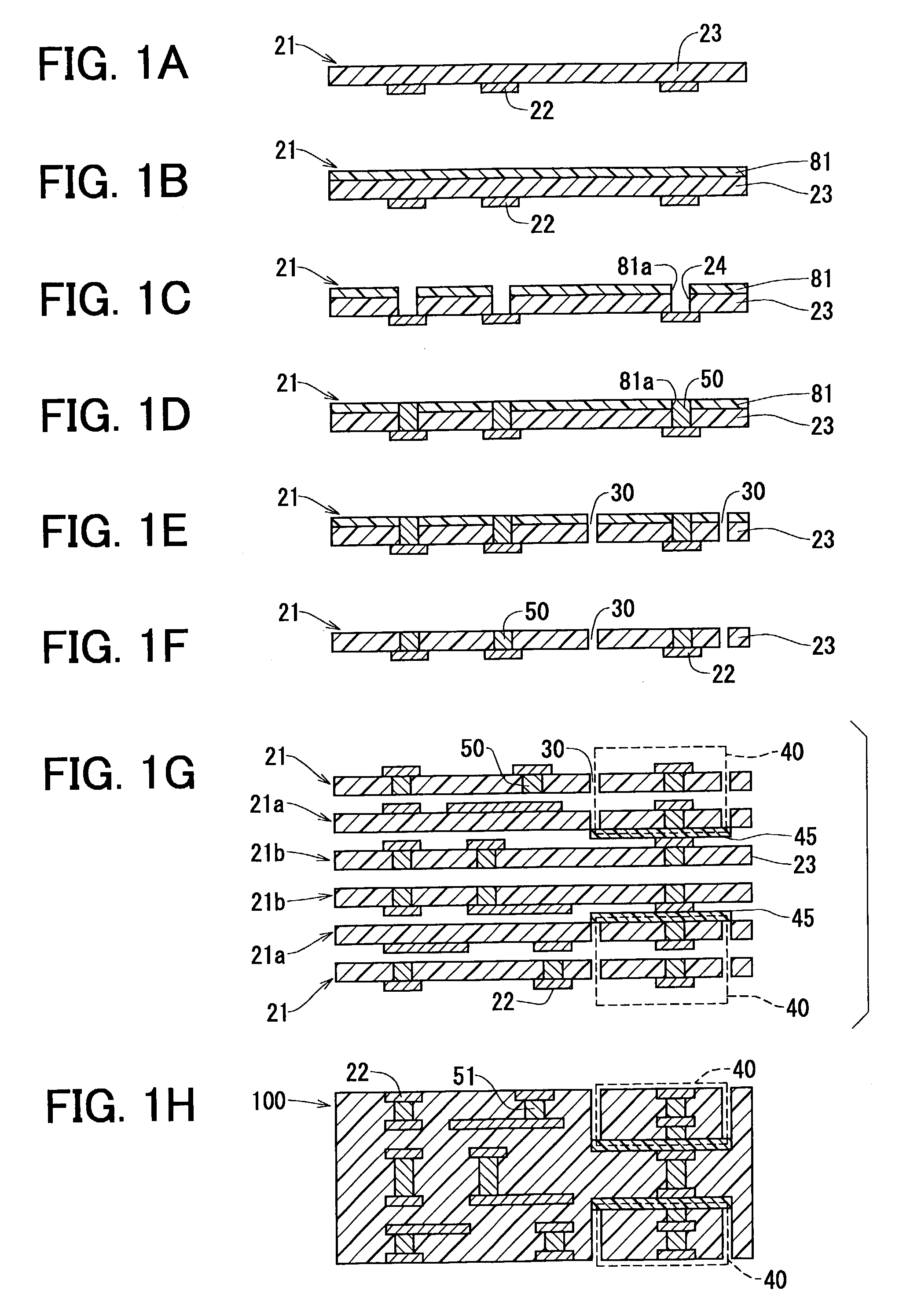
[0021]As shown in FIGS. 1A to 1H, a multi-layer printed circuit board 100 is manufactured. First, a conductive foil is formed on one side surface of a resin film 23. Then, the conductive foil on the resin film 23 is etched to have a conductive circuit 22 with a predetermined pattern so that a one-side printed film 21 is formed. In the first embodiment, for example, the conductive foil is composed of a copper foil having the thickness of 18 μm. The resin film 23 is composed of thermoplastic resin, which is made of polyether ether ketone resin (i.e., PEEK resin) and polyether imide resin (i.e., PEI resin). The weight percentage of the PEEK resin is about 35–65 wt. %, and the weight percentage of the PEI resin is about 65–35 wt. %, in accordance with the weight percentage of the PEEK resin. The thickness of the resin film 23 is about 25–75 μm.
[0022]After the conductive circuit 22 is formed in FIG. 1A, as shown in FIG. 1B, a passivation film 81 (protection film) ...
second embodiment
[0046](Second Embodiment)
[0047]In the second embodiment, as shown in FIG. 6A, plural one-side printed films 21, 21c are stacked to form stacked films, similar to the first embodiment. The one-side printed films 21,21c are formed by the same manner as the first embodiment. However, the two one-side printed films 21 do not have a slit, and the four one-side printed films 21c have slits 31 that are positioned at the same position in the films 21c. No separation sheet is inserted between the one-side printed films 21, 21c.
[0048]After the six one-side printed films 21, 21c are stacked to form the stacked films, a linked slit 32 with a predetermined width is formed in the first to fourth layer one-side printed films 21c. Then, the stacked films are pressurized and heated in vacuum. Therefore, as shown in FIG. 6B, the one-side printed films 21, 21c are bonded to each other. Moreover, in this pressurizing and heating process, a conductive paste 50 in the hole 24 is sintered and integrated ...
third embodiment
[0050](Third Embodiment)
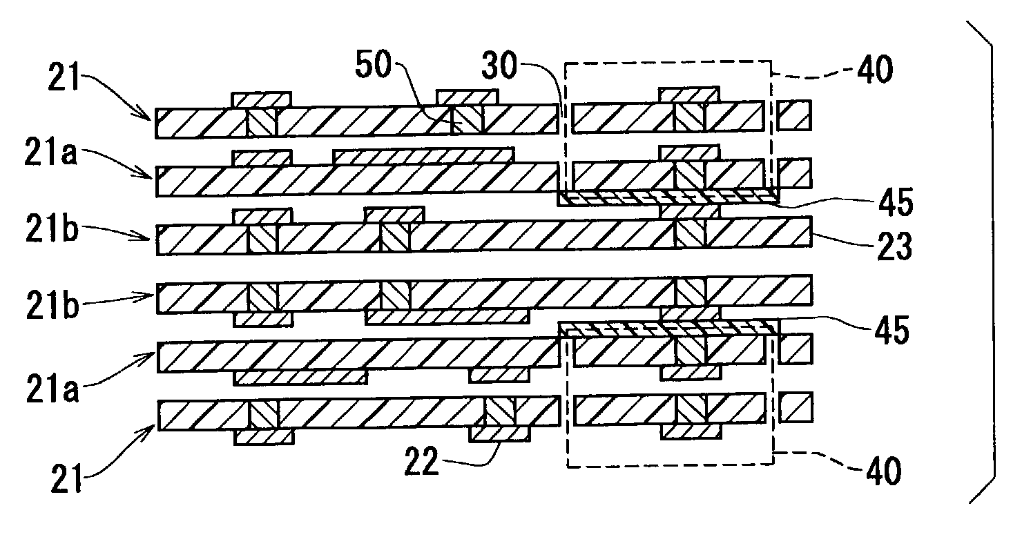
[0051]At first, the one-side printed film 21 is prepared in the same manner as the first embodiment. After the passivation film 81 is stripped and eliminated from the one-side printed film 21, plural one-side printed films 21, 21a, 21b are stacked integrally, as shown in FIG. 9A. For example, six one-side printed films 21, 21a, 21b are stacked. In the first layer, a copper foil 62 is formed on the top surface of the one-side printed film 21. In the second layer, the conductive circuit 22 is formed on the top surface of the one-side printed film 21a and the separation sheet 45 is formed on the bottom surface of the one-side printed film 21a. In the third layer, the conductive circuit 22 is formed on the top surface of the one-side printed film 21b. In the fourth layer, the conductive circuit 22 is formed on the top surface of the one-side printed film 21a and the separation sheet 45 is formed on the bottom surface of the one-side printed film 21a. In the fifth...
PUM
| Property | Measurement | Unit |
|---|---|---|
| Thickness | aaaaa | aaaaa |
| Shape | aaaaa | aaaaa |
| Electrical conductor | aaaaa | aaaaa |
Abstract
Description
Claims
Application Information
 - R&D
- Intellectual Property
- Life Sciences
- Materials
- Tech Scout
- Unparalleled Data Quality
- Higher Quality Content
- 60% Fewer Hallucinations
Browse by: Latest US Patents, China's latest patents, Technical Efficacy Thesaurus, Application Domain, Technology Topic, Popular Technical Reports.
© 2025 PatSnap. All rights reserved.Legal|Privacy policy|Modern Slavery Act Transparency Statement|Sitemap|About US| Contact US: help@patsnap.com


