
Magnetoresistive element, magnetic memory cell, and magnetic memory device, and method for manufacturing the same

a technology of magnetic memory cell and magnetic memory device, which is applied in the direction of digital storage, semiconductor devices, instruments, etc., can solve the problems of unstable magnetic direction of storing information, difficult to hold recorded information, and not disclose a concrete method for manufacturing tmr-mram having the structure. , to achieve the effect of high precision, stable writing and efficient us

Inactive Publication Date: 2006-04-11
TDK CORPARATION
View PDF17 Cites 7 Cited by
  • Summary
  • Abstract
  • Description
  • Claims
  • Application Information

AI Technical Summary

Benefits of technology

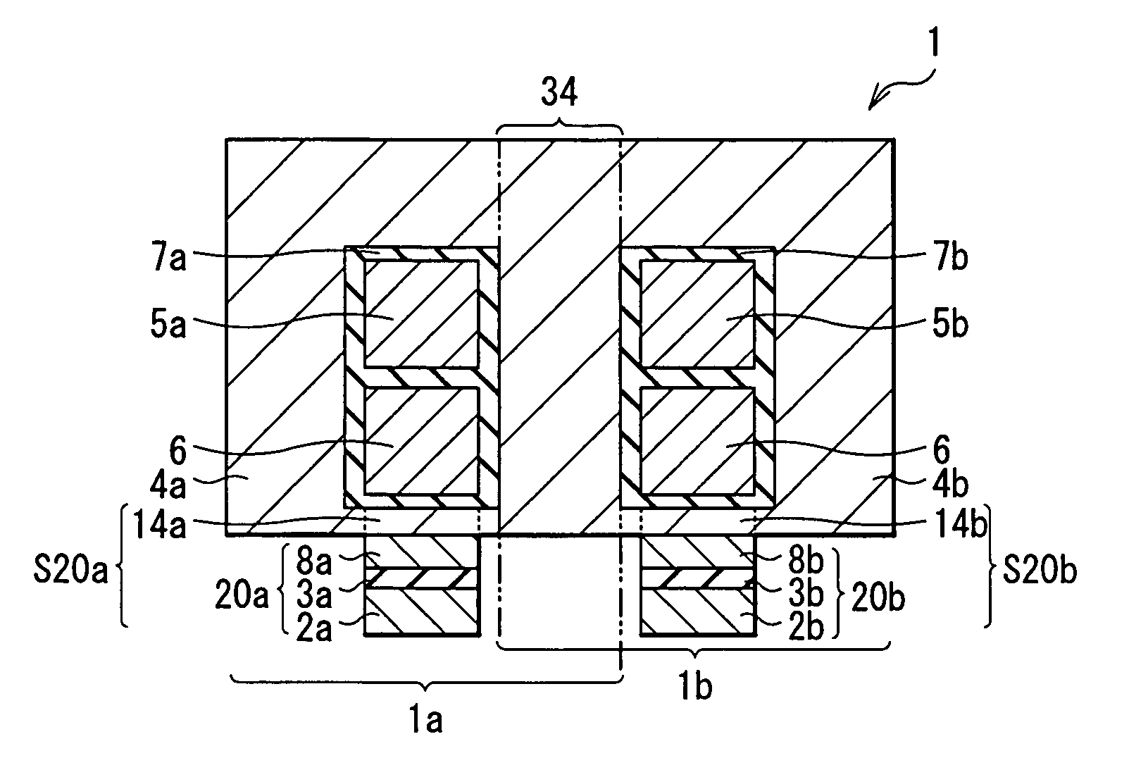
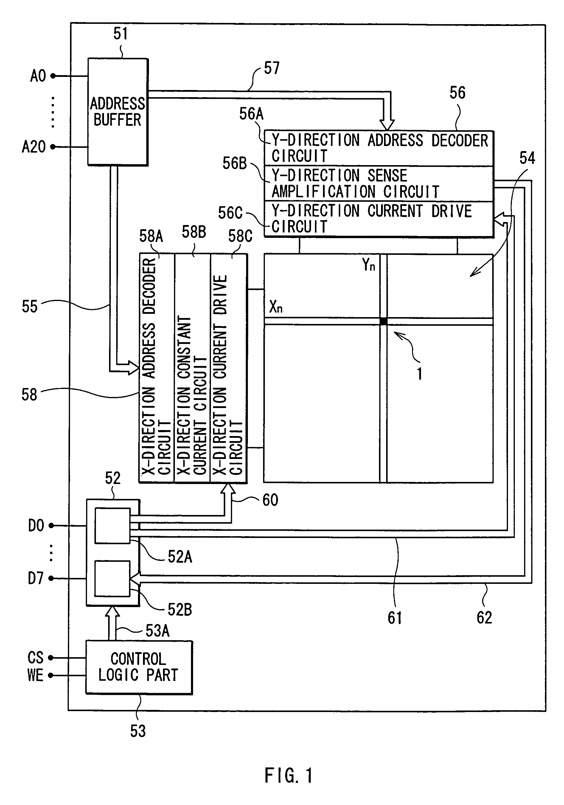
[0010]The present invention has been achieved in consideration of such problems and its first object is to provide a magneto-resistive element, a magnetic memory cell, and a magnetic memory device including the magneto-resistive element and the magnetic memory cell, each having a compact configuration, to which information can be stably written by efficiently using a magnetic field generated by current flowing in a conductor, and which is formed with high precision. A second object is to provide a method of manufacturing the magneto-resistive element, a magnetic memory cell, and a magnetic memory device.
[0018]In the magnetoresistive element, magnetic memory cell, and magnetic memory devices according to the first and second aspect of the invention, at least a part of the magnetic yoke is formed by a plating film. Consequently, as compared with the case of formation by a dry film forming method, relatively large thickness and higher dimensional precision can be obtained.
[0019]In the method of manufacturing the magnetoresistive element and the method of manufacturing the magnetic memory cell according to the invention, and the method of manufacturing the magnetic memory device according to the second aspect of the invention, at least a part of the magnetic yoke is formed by a plating film. Consequently, as compared with the case of formation by a dry film forming method, relatively larger thickness and higher dimensional precision can be obtained.

Problems solved by technology

As the TMR element is becoming finer, due to the influence of a demagnetizing field generated by magnetic poles at both ends of the TMR element, the magnetization direction in a magnetic layer (free magnetization direction layer) for storing information becomes unstable and it becomes difficult to hold recorded information.
Japanese Patent Laid-open No. 2001-273759, however, does not disclose a concrete method of manufacturing the TMR-MRAM having the structure in which the closed magnetic circuit is formed.

Method used


Image

  • Magnetoresistive element, magnetic memory cell, and magnetic memory device, and method for manufacturing the same
  • Magnetoresistive element, magnetic memory cell, and magnetic memory device, and method for manufacturing the same
  • Magnetoresistive element, magnetic memory cell, and magnetic memory device, and method for manufacturing the same

Examples


examples

[0126]Concrete examples in the embodiment will now be described.

[0127]First, the inclination angle θ of the end face in the film to be patterned which is made of NiFe and formed by the frame plating method of the embodiment and that formed by the dry film forming method were compared with each other. FIG. 28A shows the result.

[0128]The lateral axis in FIG. 28A indicates average thickness Tave. (nm) of a film PF to be patterned, and the vertical axis indicates the inclination angle θ(deg.) of the end face of the film PF to be patterned. The inclination angle θ is, as shown in FIG. 28B, an angle formed by a supporting face 131S on which the film PF to be patterned is formed and the end face of the film PF to be patterned. When the inclination angle θ is 0°, it means that the end face is parallel with the supporting face 131S. When the inclination angle θ is 90°, it means that the end face is perpendicular to the supporting face 131S. “◯” shows the characteristic value of a sample form...


PUM


Abstract

The present invention provides a magnetic memory device capable of performing stable operation efficiently using a magnetic field generated by write current and formed with high precision while realizing a compact configuration. Since a plating film is used for at least a part of a magnetic yoke, as compared with the case of formation by a dry film forming method, sufficient thickness and higher dimensional precision can be obtained. Consequently, a more stabilized return magnetic field can be generated and high reliability can be assured. Neighboring memory cells can be disposed at narrower intervals, so that the invention is suitable for realizing higher integration and higher packing density.

Description

BACKGROUND OF THE INVENTION[0001]1. Field of the Invention[0002]The present invention relates to a magnetoresistive element and a magnetic memory cell each including a magneto-sensitive layer of which magnetization direction changes according to an external magnetic field and a method of manufacturing the same. The invention also relates to a magnetic memory device for recording / reading information by using a change in the magnetization direction of a magneto-sensitive layer in the magnetoresistive element and the magnetic memory cell and to a method of manufacturing the same.[0003]2. Description of the Related Art[0004]Conventionally, as general memories used for an information processor such as a computer or a communication device, volatile memories such as a DRAM (Dynamic Random Access Memory) and an SRAM (Static RAM) are used. The volatile memories have to be refreshed by always supplying current to hold stored information. When the power source is turned off, all of information...

Claims


Application Information

Patent Timeline
Patent Type & Authority Patents(United States)
IPC IPC(8): H01L29/76G11C11/15G11C11/00G11C11/16H01L21/8246H01L27/105H01L27/22H01L43/08H01L43/12
CPCG11C11/16H01L27/224H01L43/12H01L43/08H01L27/226H10B61/20H10B61/10H10N50/10H10N50/01
Inventor KAMIJIMA, AKIFUMIHATATE, HITOSHI
Owner TDK CORPARATION
Learn More