Delay circuit that scales with clock cycle time

a delay circuit and clock cycle technology, applied in the field of electronic circuits, can solve the problems of inability to easily adjust in proportion to input signals, inability to propagate delay of this element, and inability to control etc., to achieve the effect of controlling accurately across pvt variations and lowering process variation

Active Publication Date: 2006-03-28
MONTEREY RES LLC
View PDF11 Cites 15 Cited by
  • Summary
  • Abstract
  • Description
  • Claims
  • Application Information

AI Technical Summary

Benefits of technology

[0008]Thus, a need exists for a circuit having a delay element that does not vary with PVT variations. The circuit may have a propagation delay that does not depend on a fixed resistor value, but rather has a propagation delay as a function of a capacitance ratio that can be controlled very accurately across PVT variations. A further need exists for a delay element that is scalable according to an input clock cycle. Still another need exists for a delay element which is compatible with existing manufacturing and operating processes. Embodiments of the present invention provide these advantages.
[0012]In its various embodiments, the present invention provides a circuit having a process, voltage, and temperature (PVT) invariant delay element. The present invention also provides a circuit having a delay element wherein the propagation delay does not depend on a fixed resistor value, but where the propagation delay is a function of a capacitance ratio which can be controlled accurately across PVT variations. The present invention further provides a circuit having a PVT invariant delay element which is scalable according to the input clock cycle. The present invention additionally provides a circuit having a PVT invariant delay element which achieves the above accomplishments and which readily interfaces with industry standard components and meets industry standard specifications.

Problems solved by technology

A disadvantage of this conventional circuit 100 is that the wide variation in propagation delay across PVT may cause improper operation of the application.
A further disadvantage of this conventional circuit 100 is that the propagation delay of this element (which depends only on the resistance and input capacitance values of the circuit), once designed, does not readily adjust in proportion to an input signal.

Method used


Image

  • Delay circuit that scales with clock cycle time
  • Delay circuit that scales with clock cycle time
  • Delay circuit that scales with clock cycle time

Examples


Embodiment Construction

[0018]Reference will now be made in detail to embodiments of the invention, examples of which are illustrated in the accompanying drawings. While the invention will be described in conjunction with the preferred embodiments, it will be understood that they are not intended to limit the invention to these embodiments. On the contrary, the invention is intended to cover alternatives, modifications and equivalents, which may be included within the spirit and scope of the invention as defined by the appended claims. Furthermore, in the following detailed description of the present invention, numerous specific details are set forth in order to provide a thorough understanding of the present invention. However, the present invention may be practiced without these specific details. In other instances, well-known methods, procedures, components, and circuits have not been described in detail as not to unnecessarily obscure aspects of the present invention.

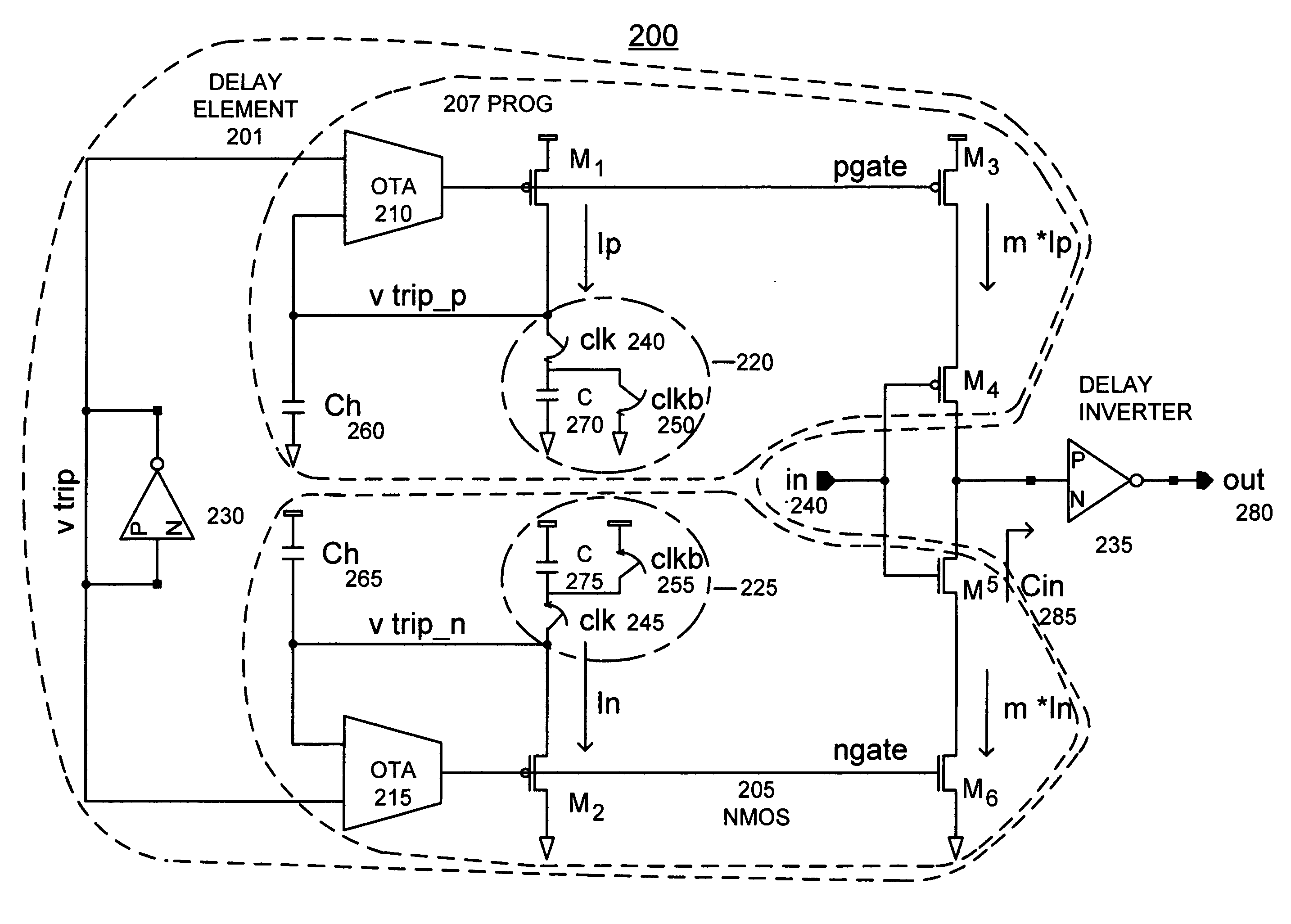
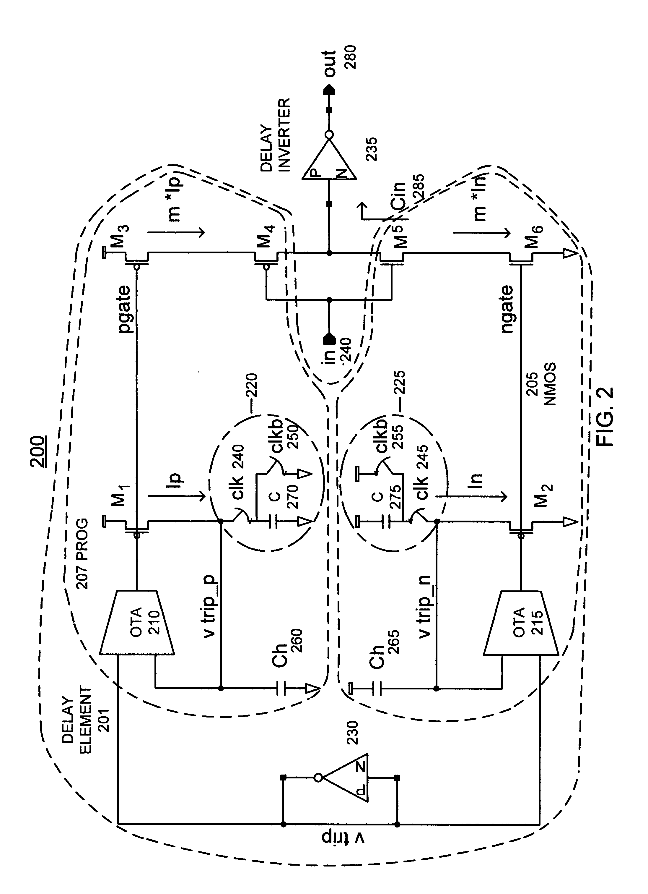
[0019]With reference now to FIG. 2,...


PUM


Abstract

A circuit having a process, voltage, and temperature (PVT) invariant delay element is disclosed. In one embodiment, the present invention includes a first and second operational transconductance amplifier (OTA), a first and second switched capacitor driven by a clock, and a first and second clock-controlled switch. In addition, the present invention includes a trip inverter, a delay inverter, and a plurality of transistors. In so coupling the first and second OTA, the first and second switched capacitor, the first and second clock-controlled switch, the trip inverter, the delay inverter, and the plurality of transistors, a circuit having a PVT invariant delay element is provided.

Description

RELATED U.S. APPLICATION[0001]This application claims priority to the provisional patent application, Ser. No. 60 / 457,525, entitled “A Switched Capacitor Delay Element with Minimum Delay Variation Across PVT,” with filing date Mar. 24, 2003 now abandoned, and assigned to the assignee of the present application. This application is hereby incorporated by reference.FIELD OF THE INVENTION[0002]The present invention relates generally to electronic circuitry and in particular to circuits having PVT invariant delays.BACKGROUND OF THE INVENTION[0003]Delay element circuits are widely used in analog and digital electronic circuitry. The purpose of such a circuit is to take an input signal, to delay it for a period of time, and to then pass the signal to an output circuit. Delay element circuits may be used to adjust the setup (ts) and hold (th) times of signals entering a circuit, or to adjust the clock to output time (sometimes referred to as tCO or tCQ) of signals leaving a circuit. Delay ...

Claims


Application Information

Patent Timeline
IPC IPC(8): H03H11/26
CPCH03H11/265
Inventor SANCHETI, SANJAY K.CHEN, SUWEI
Owner MONTEREY RES LLC
Why Eureka
Try Eureka