Pixel structure of display array substrate and display device using the same

a technology of display array substrate and pixel structure, which is applied in static indicating devices, instruments, non-linear optics, etc., can solve the problems of unstable transmittance, relative difficulty in controlling the line width of the indium tin oxide (ito) slit in the exposure, development, etching process, etc., and achieves the improvement of pixels of the pixel array display screen of the display array substrate, reducing the sensitivity to process variation, and reducing the effect of brightness differen

Active Publication Date: 2019-08-13
HKC CORP LTD +1
View PDF11 Cites 0 Cited by
  • Summary
  • Abstract
  • Description
  • Claims
  • Application Information

AI Technical Summary

Benefits of technology

[0003]To resolve the foregoing technical problem, an objective of this application is to provide a pixel structure of display array substrate, thereby effectively resolving a mura problem, and mitigating a brightness difference caused by a variation in an ITO slit of a fourth subpixel.
[0017]A beneficial effect of this application is: pixels of a pixel array display screen of a display array substrate are improved, and therefore insensitivity to a process variation is achieved. For a problem extended from a novel process of a pixel array of a display array substrate, this design provides a method for feeding back, correcting, and compensating for a line width, thereby mitigating a brightness difference caused by an ITO slit of a fourth subpixel.

Problems solved by technology

In the process, because of a severe segment difference of a subpixel (because of a width drop of a flat layer), it is relatively difficult to control a line width of an indium tin oxide (ITO) slit in a process of exposure, development, and etching.
Therefore, a problem of unstable transmittance is easily caused.

Method used


Image

  • Pixel structure of display array substrate and display device using the same
  • Pixel structure of display array substrate and display device using the same
  • Pixel structure of display array substrate and display device using the same

Examples


Embodiment Construction

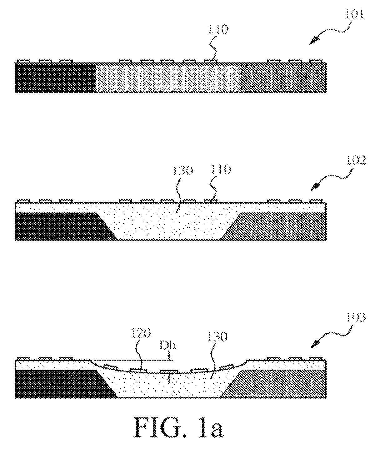
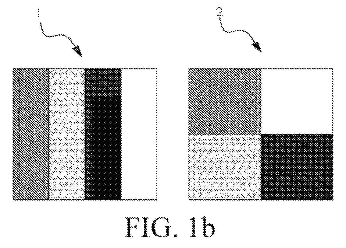
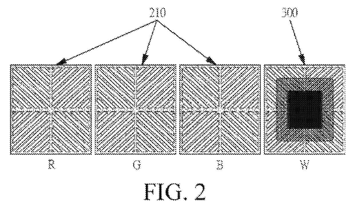
[0033]The following embodiments are described with reference to the accompanying drawings used to exemplify specific embodiments for implementation of this application. Terms about directions mentioned in this application, such as “on”, “below”, “front”, “back”, “left”, “right”, “in”, “out”, and “side surface” merely refer to directions of the accompanying drawings. Therefore, the used terms about directions are used to describe and understand this application, and are not intended to limit this application.

[0034]The accompanying drawings and the description are considered to be essentially exemplary, rather than limitative. In figures, units with similar structures are represented by using a same reference number. In addition, for understanding and ease of description, a size and a thickness of each component shown in the accompanying drawings are arbitrarily shown, but this application is not limited thereto.

[0035]In the accompanying drawings, for clarity, thicknesses of a layer, ...


PUM

PropertyMeasurementUnit
brightnessaaaaaaaaaa
widthsaaaaaaaaaa
line widthaaaaaaaaaa

Abstract

This application provides a pixel structure of display array substrate and a display device applied thereto. The pixel structure of display array substrate includes a plurality of pixel units arranged in an array manner. Each pixel unit includes a first subpixel, a second subpixel, and a fourth subpixel. Each pixel unit further includes: a first subpixel electrode and a second subpixel electrode, respectively located in the first subpixel and the second subpixel; and a fourth subpixel electrode, where the fourth subpixel electrode includes a first pixel electrode, a second pixel electrode, a third pixel electrode, and a fourth pixel electrode located in four areas of the fourth subpixel, respectively, and each the first pixel electrode, the second pixel electrode, the third pixel electrode, and the fourth pixel electrode are divided into at least two compensation area.

Description

BACKGROUNDTechnical Field[0001]This application relates to an electrode design method, and in particular, to a pixel structure of display array substrate and a display device applied thereto.Related Art[0002]Generally, mura is caused by uneven brightness distribution on a display screen. In a pixel design of a vertical alignment (VA) type / in-plane switching (IPS) type / fringe field switching (FFS) type, a pixel electrode is generally designed to have a slit form, and control of a line width of the pixel electrode greatly affects liquid crystal efficiency. In a process of a pixel design of a display array substrate, a segment difference may occur between subpixels having different colors. In the process, because of a severe segment difference of a subpixel (because of a width drop of a flat layer), it is relatively difficult to control a line width of an indium tin oxide (ITO) slit in a process of exposure, development, and etching. Therefore, a problem of unstable transmittance is ea...

Claims


Application Information

Patent Timeline
Patent Type & Authority Patents(United States)
IPC IPC(8): G02F1/1337G02F1/1343G02F1/1362G02F1/1335
CPCG02F1/133707G02F1/134309G02F1/136286G09G2320/0233G02F2201/123G09G2300/0439G02F1/133528G02F2201/52
Inventor CHEN, YU-JEN
Owner HKC CORP LTD
Why Eureka
Try Eureka