Particle detector assembly
- Summary
- Abstract
- Description
- Claims
- Application Information
AI Technical Summary
Benefits of technology
Problems solved by technology
Method used
Image
Examples
Embodiment Construction
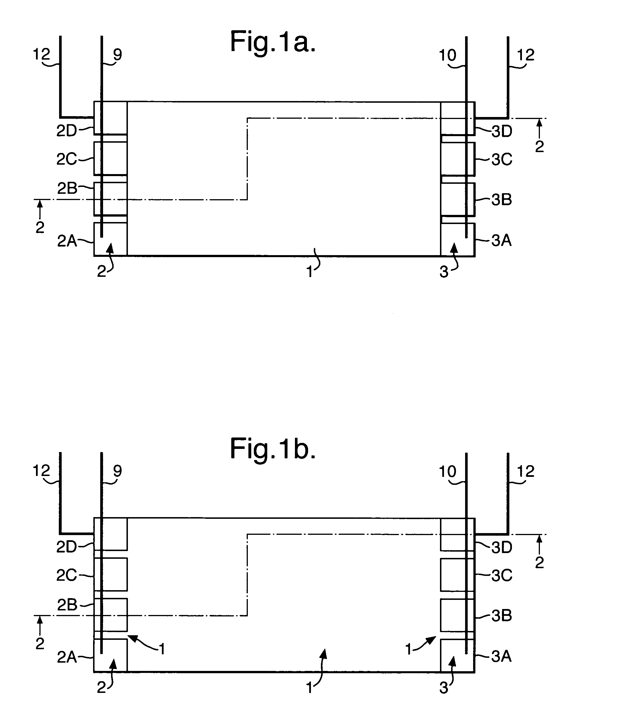
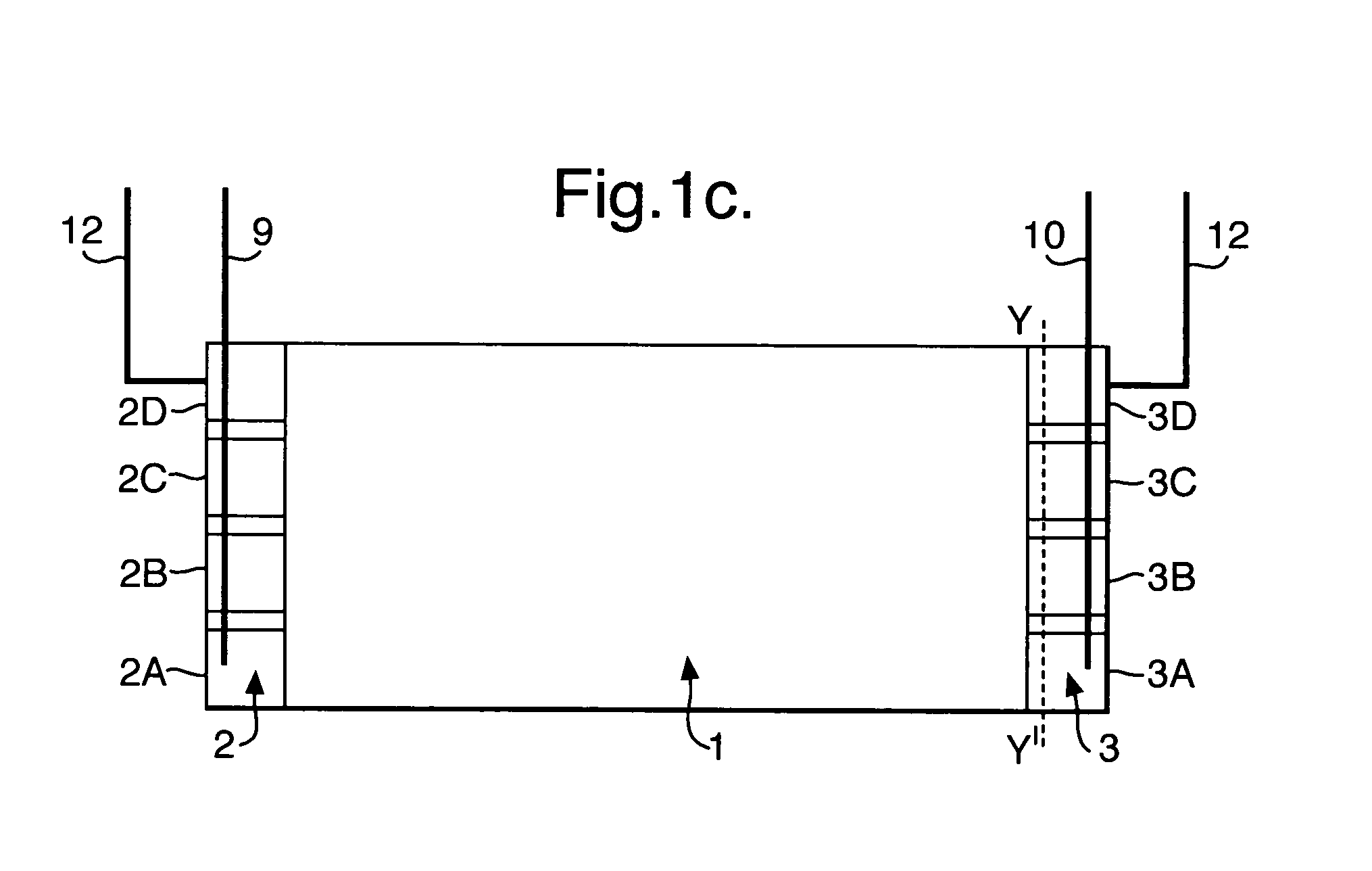
[0021]FIG. 1a illustrates a first example of the assembly in plan view and this comprises a superconducting Ta absorber 1 to which is mounted two STJ detectors 2,3, each detector comprising an array of parallel connected STJ devices 2A–2D and 3A–3D respectively. Of course, any other known absorber material could be used such as Al, Ti, V, Nb, etc. Further, although each detector comprises four devices in this example, three or more, preferably many more, could be used.
[0022]The construction of the devices shown in FIG. 1a is illustrated in more detail in FIG. 2a. As can be seen in FIG. 2a the Ta absorber (absorber film) 1, typically having an area of about 250×500 μm2 or more is provided on a sapphire substrate 4. Each STJ device 2,3 comprises an insulating barrier 5, such as AIOx, sandwiched between a pair of quasiparticle traps 6, typically A1 having a thickness of 30–200 nm (or another superconductor having a smaller superconducting gap than the absorbing film). A Ta top electrod...
PUM
 Abstract
Description
Claims
Application Information
 - R&D
- Intellectual Property
- Life Sciences
- Materials
- Tech Scout
- Unparalleled Data Quality
- Higher Quality Content
- 60% Fewer Hallucinations
Browse by: Latest US Patents, China's latest patents, Technical Efficacy Thesaurus, Application Domain, Technology Topic, Popular Technical Reports.
© 2025 PatSnap. All rights reserved.Legal|Privacy policy|Modern Slavery Act Transparency Statement|Sitemap|About US| Contact US: help@patsnap.com


