Wireless communication system
a communication system and wireless technology, applied in the direction of low noise amplifiers, power management, amplifiers with min 3 electrodes or 2 pn junctions, etc., can solve the problem of no wiring arrangement between the electrode terminals and the side of mounting the semiconductor chip, and achieve the effect of enhancing the gain and noise characteristi
- Summary
- Abstract
- Description
- Claims
- Application Information
AI Technical Summary
Benefits of technology
Problems solved by technology
Method used
Image
Examples
first embodiment
(First Embodiment)
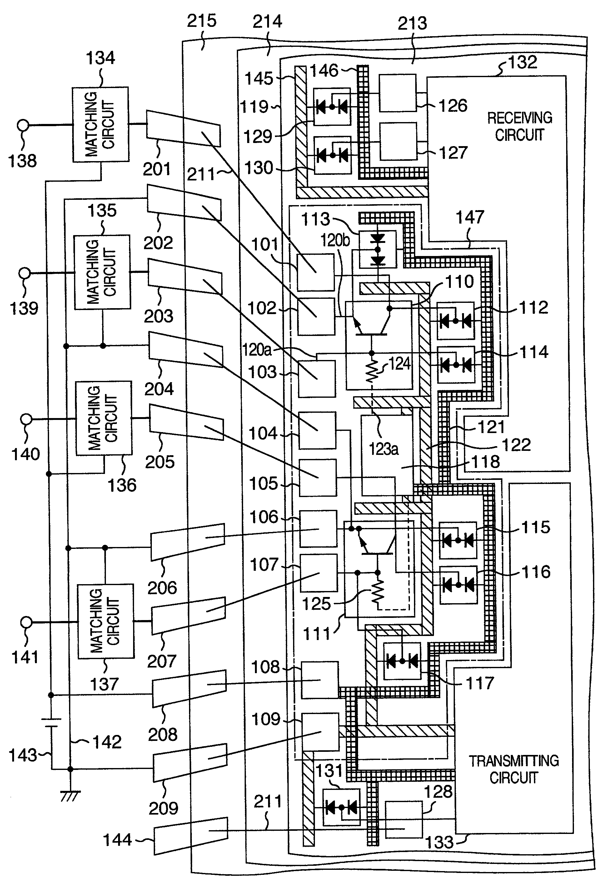
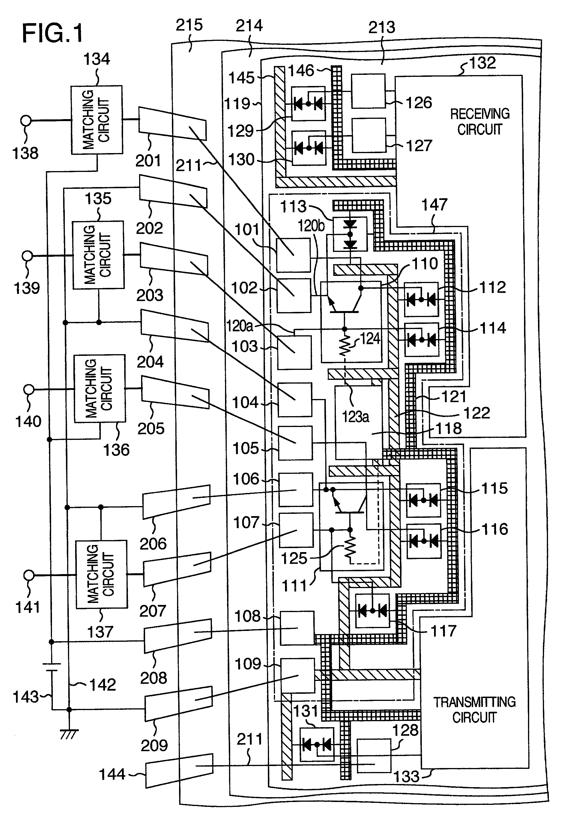
[0040]FIGS. 1 to 7 are figures each of which relates to a wireless communication system according to a first embodiment of the present invention. In the first embodiment, an example in which the present invention is applied to a wireless communication system of a TDMA (Time Division Multiple Access) system, e.g., a terminal apparatus of a wireless communication mobile body will hereinbelow be described in detail.
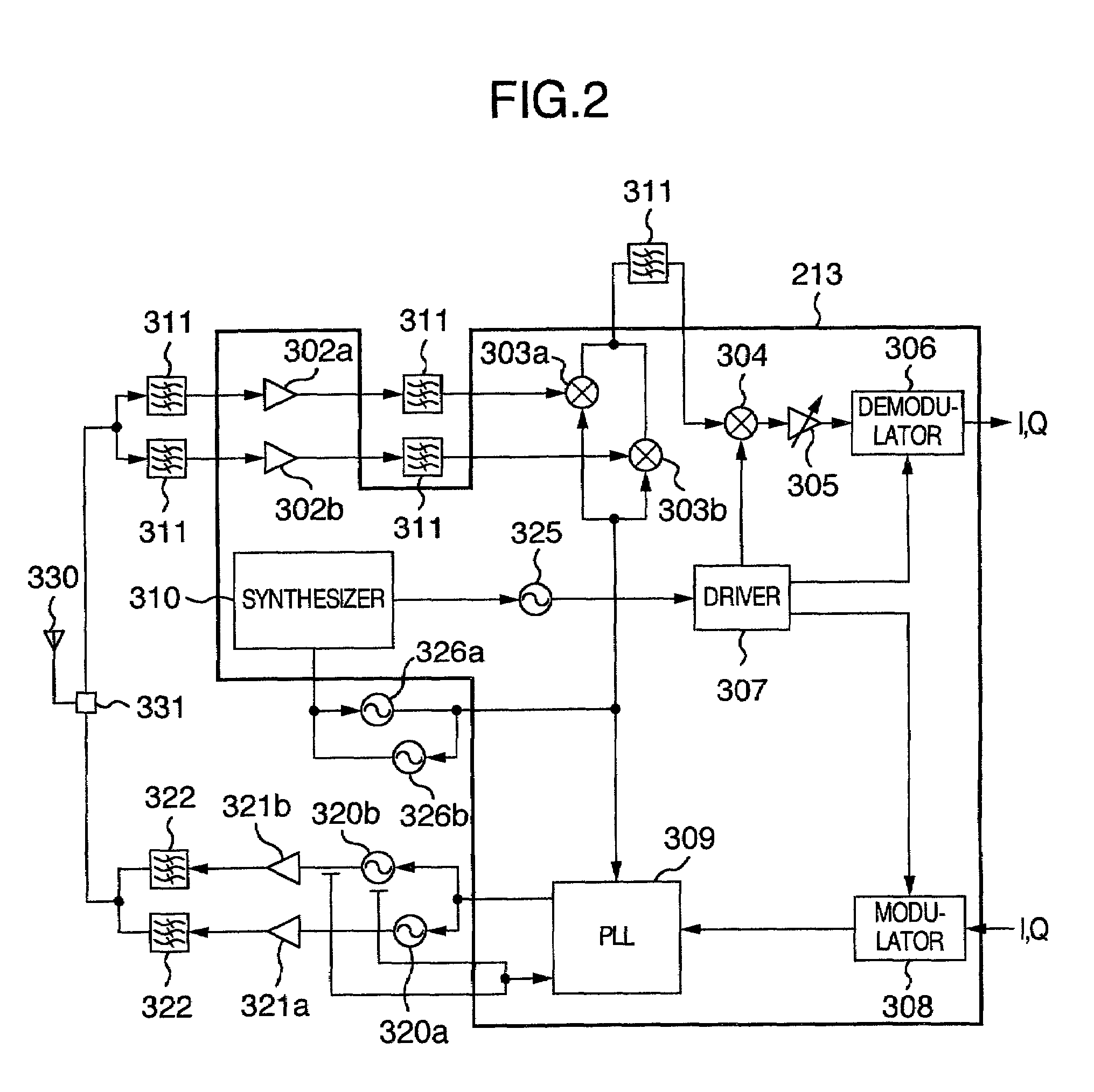
[0041]Now, a configuration of a TDMA dual band wireless communication terminal apparatus will hereinbelow be described with reference to FIG. 2. This terminal apparatus can execute the signal processing for a GSM system of a 900 MHz band and a DCS 1800 system of a 1800 MHz band.
[0042]In a block diagram shown in FIG. 2, a transmitting and receiving circuit electrically connected to an antenna 330 through a transmitting and receiving switching unit 331 are both shown and each of them is connected to a base band signal processing circuit (not shown).
[0043]The ...
third embodiment
(Third Embodiment)
[0102]FIGS. 10 and 11 show a third embodiment of the present invention. FIG. 10 is a schematic cross sectional view showing the construction of a CSP (Chip Size Package) containing a semiconductor integrated circuit device, which is incorporated in the wireless communication system, and FIG. 11 is a block diagram, partly in circuit diagram, showing the layout of a multilayer ceramic substrate and the like in which the CSP containing the semiconductor integrated circuit device is incorporated.
[0103]The CSP has the construction in which solder bumps 601 are respectively provided on the pads (not shown) of the IC chip 213; these solder bumps 601 are respectively bonded to the pads (not shown) on the surface of a multilayer ceramic substrate 603 to be attached thereto; and a filler 602 is led into the space defined between the IC chip 213 and the multilayer ceramic substrate 603 to fix the IC chip 213 to the multilayer ceramic substrate 603. In addition, the rear face ...
PUM
 Abstract
Description
Claims
Application Information
 - R&D
- Intellectual Property
- Life Sciences
- Materials
- Tech Scout
- Unparalleled Data Quality
- Higher Quality Content
- 60% Fewer Hallucinations
Browse by: Latest US Patents, China's latest patents, Technical Efficacy Thesaurus, Application Domain, Technology Topic, Popular Technical Reports.
© 2025 PatSnap. All rights reserved.Legal|Privacy policy|Modern Slavery Act Transparency Statement|Sitemap|About US| Contact US: help@patsnap.com


