
Nonvolatile memory cell with a floating gate at least partially located in a trench in a semiconductor substrate

a technology of floating gate and memory cell, which is applied in the direction of semiconductor devices, electrical devices, transistors, etc., can solve the problems of unfavorable increase of programming and erase times (or voltages), and achieve the effect of increasing the vertical fet channel width, reducing the programming time of the cell, and reducing the programming tim

Inactive Publication Date: 2006-02-28
PROMOS TECH INC
View PDF58 Cites 6 Cited by
  • Summary
  • Abstract
  • Description
  • Claims
  • Application Information

AI Technical Summary

Benefits of technology

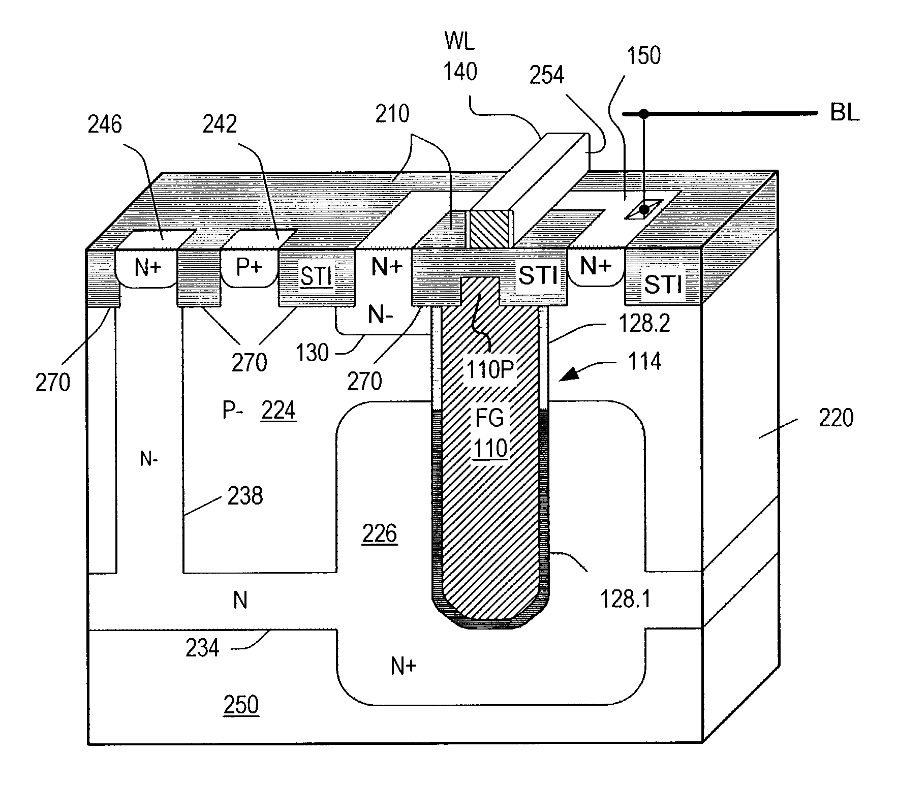
[0012]In some embodiments of the invention, a floating gate of a nonvolatile memory cell is formed in a trench as in FIG. 1, but the wordline has a portion overlying the trench. See FIG. 2A for example. This wordline positioning offers much flexibility in the memory layout. For example, the region 130 in FIG. 2A can be extended around the floating gate to increase the vertical FET channel width. A large vertical FET channel width reduces the cell's programming time if the cell is programmed by channel hot electron injection. The cell reading time can also be reduced due to a larger current through the cell.
[0013]In some embodiments of the present invention, the dielectric lining the trench is stronger against leakage near one of the source / drain regions of the floating gate transistor than near the channel region. For example, in FIG. 2A, the dielectric lining the trench has a bottom portion 128.1 near the bottom source / drain region 226 and has a portion 128.2 near the channel region. Bottom portion 128.1 is stronger against leakage than the portion 128.2. “Stronger” means the leakage per unit area is smaller at a given voltage across the dielectric. As is well known, small leakage improves data retention but undesirably increases the programming and erase times (or voltages). If the memory is not programmed or erased through the bottom source / drain region, the stronger dielectric near this region improves data retention without increasing the programming and erase times or voltages.
[0014]In some embodiments, additional dielectric is provided between the trench and a top part of a source / drain region of the floating gate transistor. For example, in FIG. 2A, the additional dielectric is a portion of dielectric 210 extending below the top surface of the substrate between the trench 114 and the top part of source / drain region 130. Region 130 passes under the dielectric 210 to meet the trench 114. The additional dielectric reduces the capacitance between the region 130 and the floating gate. The additional dielectric can be part of a field dielectric layer, i.e. the layer that isolates active areas of the integrated circuit from each other.

Problems solved by technology

As is well known, small leakage improves data retention but undesirably increases the programming and erase times (or voltages).

Method used


Image

  • Nonvolatile memory cell with a floating gate at least partially located in a trench in a semiconductor substrate
  • Nonvolatile memory cell with a floating gate at least partially located in a trench in a semiconductor substrate
  • Nonvolatile memory cell with a floating gate at least partially located in a trench in a semiconductor substrate

Examples


Embodiment Construction

[0032]The embodiments described in this section illustrate but do not limit the invention. In particular, the materials, dimensions, voltage values, and fabrication processes are not limiting. Some information on the materials, processes, dimensions and other values given below is based on the inventors' knowledge of DRAM and other pertinent technologies and has not been tested for a non-volatile memory. The materials, dimensions, and other values may have to be modified based on the available fabrication technology and desired operational characteristics.

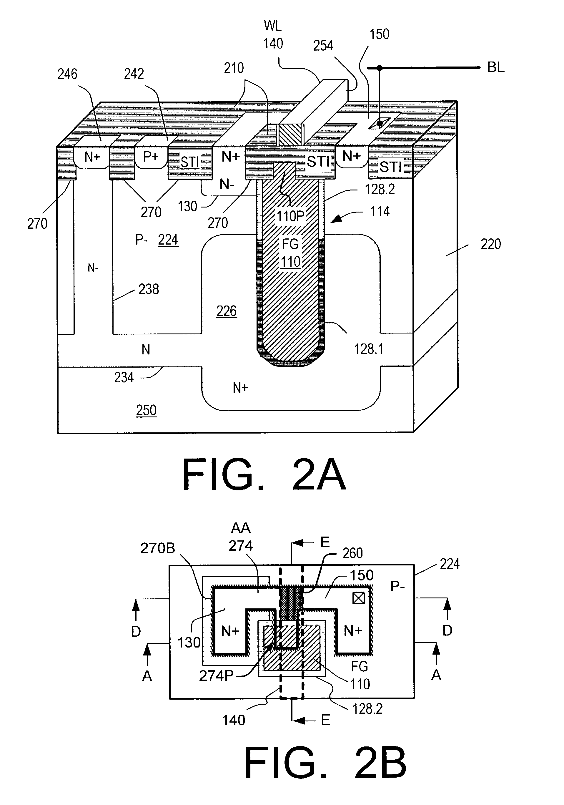
[0033]FIG. 2A shows a vertical cross section and a perspective view of an integrated circuit with a nonvolatile EEPROM memory cell. FIG. 2B is a top view, with field dielectric 210 and wordline 140 removed. The wordline boundary is shown by a dashed line. FIG. 2C is a top view with dielectric 210 present but the wordline removed. The wordline boundary, the boundary of trench 114, and the boundary of the floating gate are shown by d...


PUM


Abstract

A floating gate (110) of a nonvolatile memory cell is formed in a trench (114) in a semiconductor substrate (220). A dielectric (128) covers the surface of the trench. The wordline (140) has a portion overlying the trench. The cell's floating gate transistor has a first source / drain region (226), a channel region (224), and a second source / drain region (130). The dielectric (128) is stronger against leakage near at least a portion of the first source / drain region (122) than near at least a portion of the channel region. The stronger portion (128.1) of the additional dielectric improves data retention without increasing the programming and erase times if the programming and erase operations do not rely on a current through the stronger portion. Additional dielectric (210) has a portion located below the top surface of the substrate between the trench and a top part of the second source / drain region (130). The second source / drain region has a part located below the additional dielectric and meeting the trench. The additional dielectric can be formed with shallow trench isolation technology. The additional dielectric reduces the capacitance between the second source / drain region (130) and the floating gate.

Description

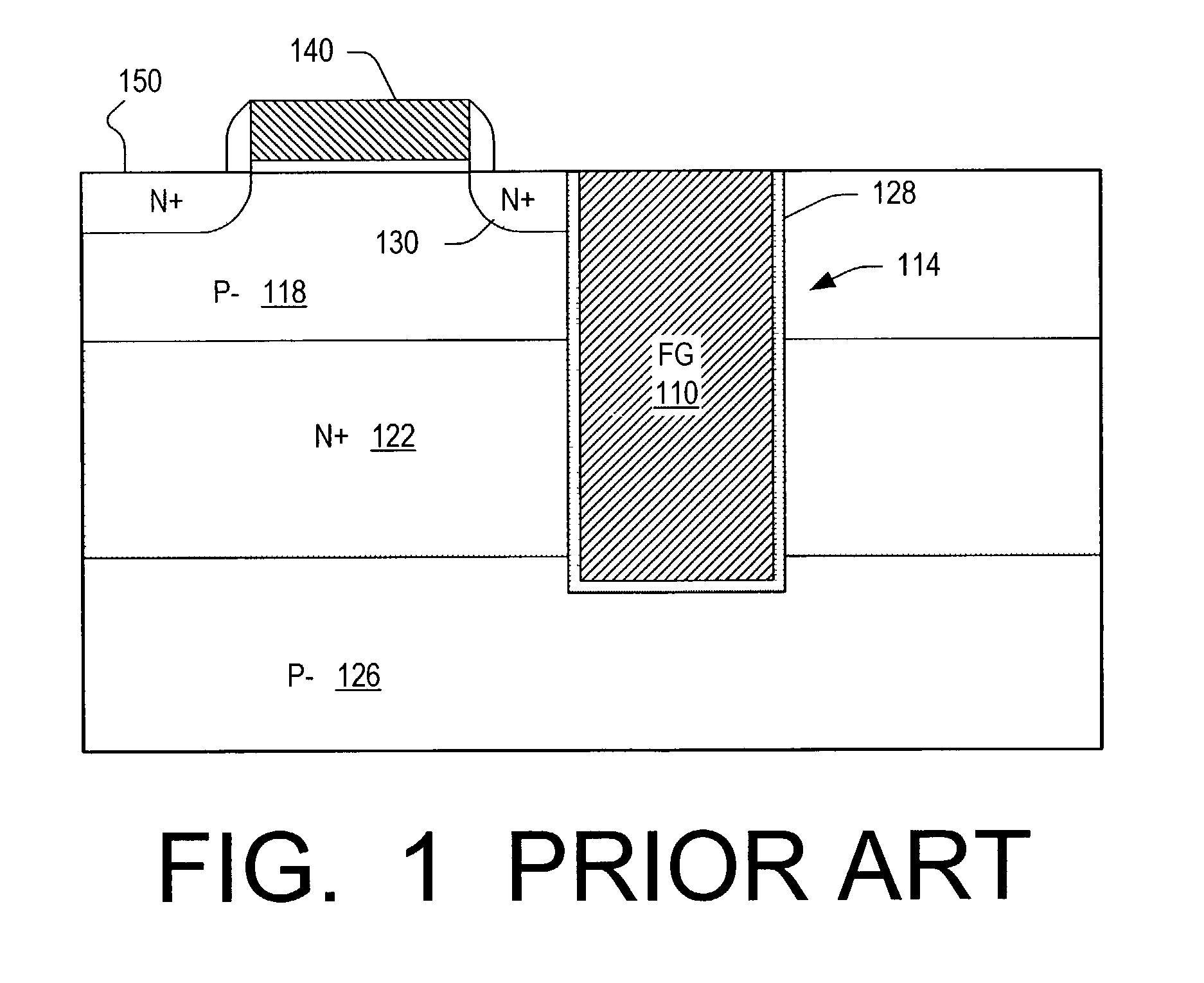
BACKGROUND OF THE INVENTION[0001]The present invention relates to nonvolatile memories.[0002]FIG. 1 illustrates a nonvolatile memory cell with a floating gate 110 located in a trench 114 formed in a semiconductor substrate. The cell is obtained by adapting a trench capacitor DRAM (dynamic random access random memory) fabrication process. See U.S. Pat. No. 5,932,908 issued Aug. 3, 1999 to Noble, entitled “TRENCH EPROM”, incorporated herein by reference. Trench 114 extends through a well 118 doped P− and a well 122 doped N+, to a region 126 doped P−. Dielectric 128 lines the trench. The capacitance of floating gate 110 is dominated by the capacitance between the floating gate and the N well 122.[0003]Floating gate 110 serves as the gate of a vertical FET (field effect transistor). The channel of this transistor is located in P well 118. The source / drain regions are provided by N well 122 and an N+ diffusion region 130 located at the top of the trench.[0004]Wordline 140 provides the ga...

Claims


Application Information

Patent Timeline
Patent Type & Authority Patents(United States)
IPC IPC(8): H01L29/788H01L21/336H01L21/8247H01L27/115H01L29/423
CPCH01L27/115H01L29/66825H01L29/42336H01L27/11521H10B69/00H10B41/30
Inventor DING, YICHAN, VEI-HAN
Owner PROMOS TECH INC
Learn More