Method of making an integrated circuit package

a technology of integrated circuits and packaging, applied in the direction of electrical equipment, semiconductor devices, semiconductor/solid-state device details, etc., can solve the problems of unreliable packages, large packages, complex bends, etc., and achieve the effect of convenient and less expensive production

Inactive Publication Date: 2006-02-28
AMKOR TECH SINGAPORE HLDG PTE LTD
View PDF373 Cites 18 Cited by
  • Summary
  • Abstract
  • Description
  • Claims
  • Application Information

AI Technical Summary

Benefits of technology

[0007]The present invention is to directed toward improved plastic packages for housing an integrated circuit die, and to leadframes and methods for making such packages. The packages of the present invention are easier and less expensive to make than conventional plastic packages, and are more reliable and efficiently-sized than conventional packages.
[0008]In one embodiment of an assembly method for a package within the present invention, Step 1 provides a metal leadframe. The leadframe includes a rectangular frame, e.g., a square frame. A substantially planar die pad is within and connected to the frame. A plurality of finger-like rectangular tabs extend from the frame toward the die pad without contacting the die pad. The number and location of the tabs around the frame may vary. The die pad and the tabs have peripheral side surfaces which include a reentrant portion(s) and asperities. The reentrant position(s) and asperities enhance the connection of the die pad and tabs to the plastic encapsulating material.

Problems solved by technology

A problem with conventional plastic packages is that their internal leadframes limit reduction of the size of the packages.
Accordingly, the packages are believed to be unreliable because the contacts could easily be pulled from the encapsulant material.
These leads are large, and have complex bends.
Including such leads in a package would increase manufacturing costs and limit reductions in the lateral size of the package.

Method used


Image

  • Method of making an integrated circuit package
  • Method of making an integrated circuit package
  • Method of making an integrated circuit package

Examples


Embodiment Construction

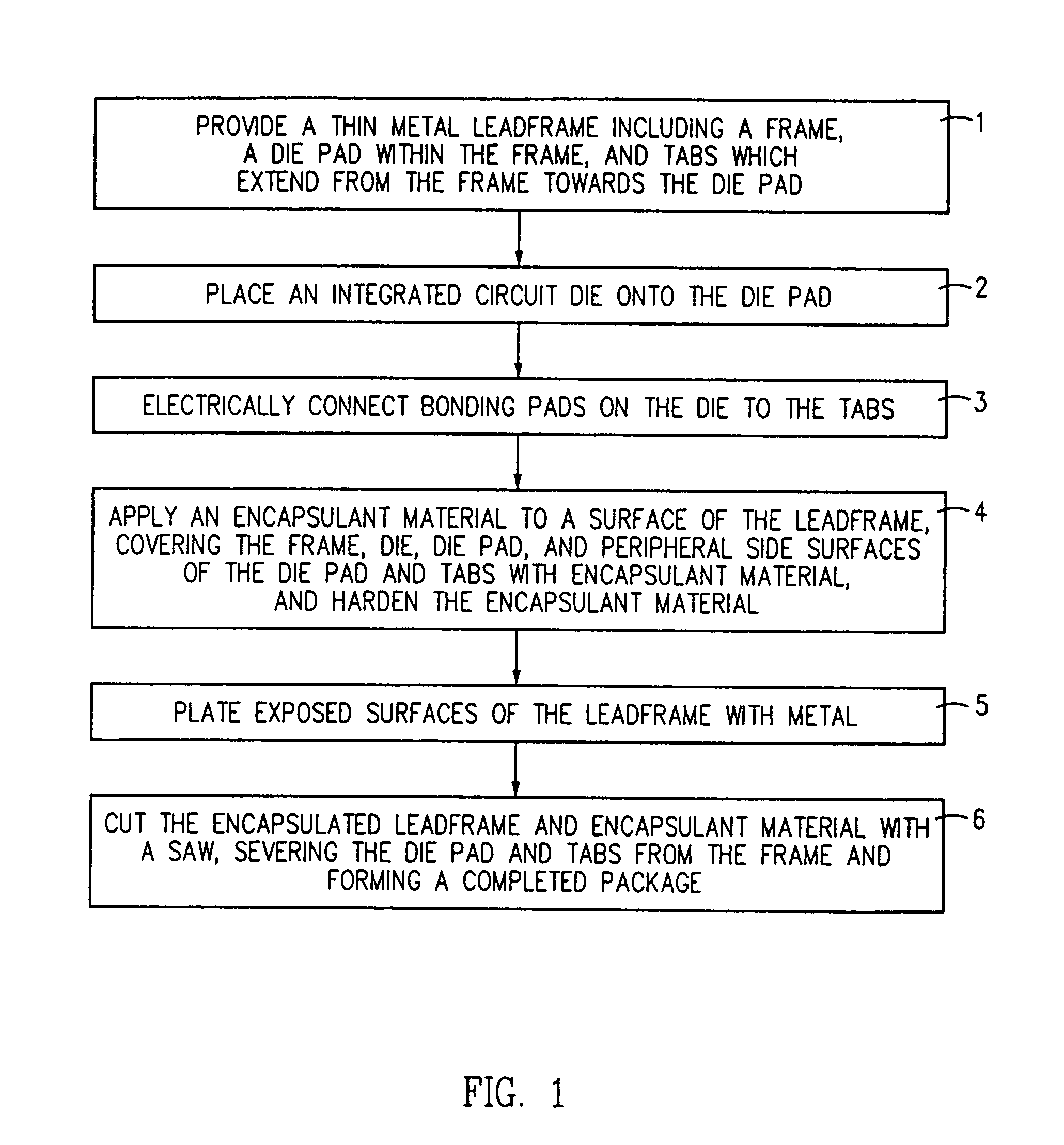
[0029]FIG. 1 shows an exemplary method of assembling a package in accordance with the present invention. FIG. 8 shows a completed package.

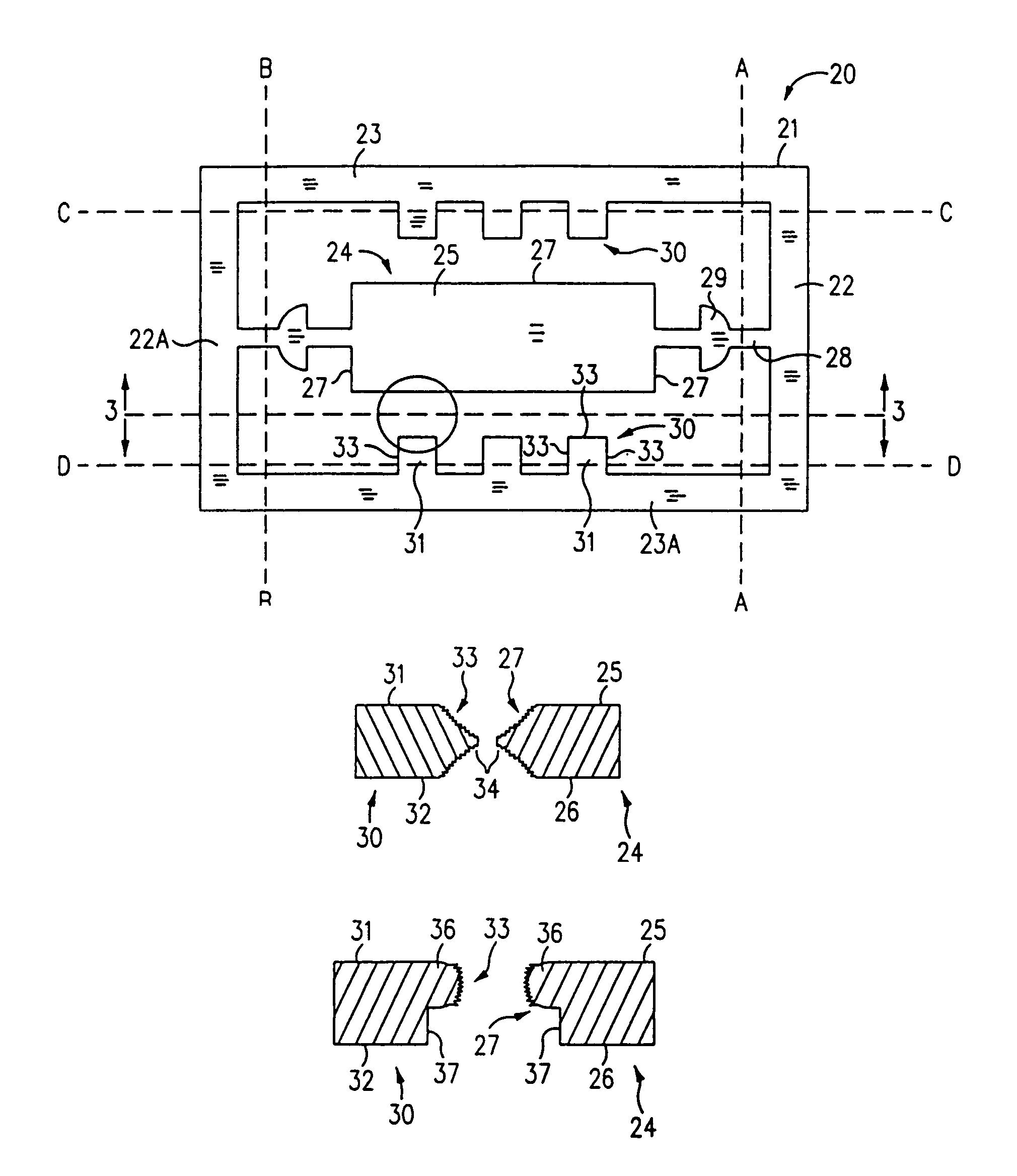
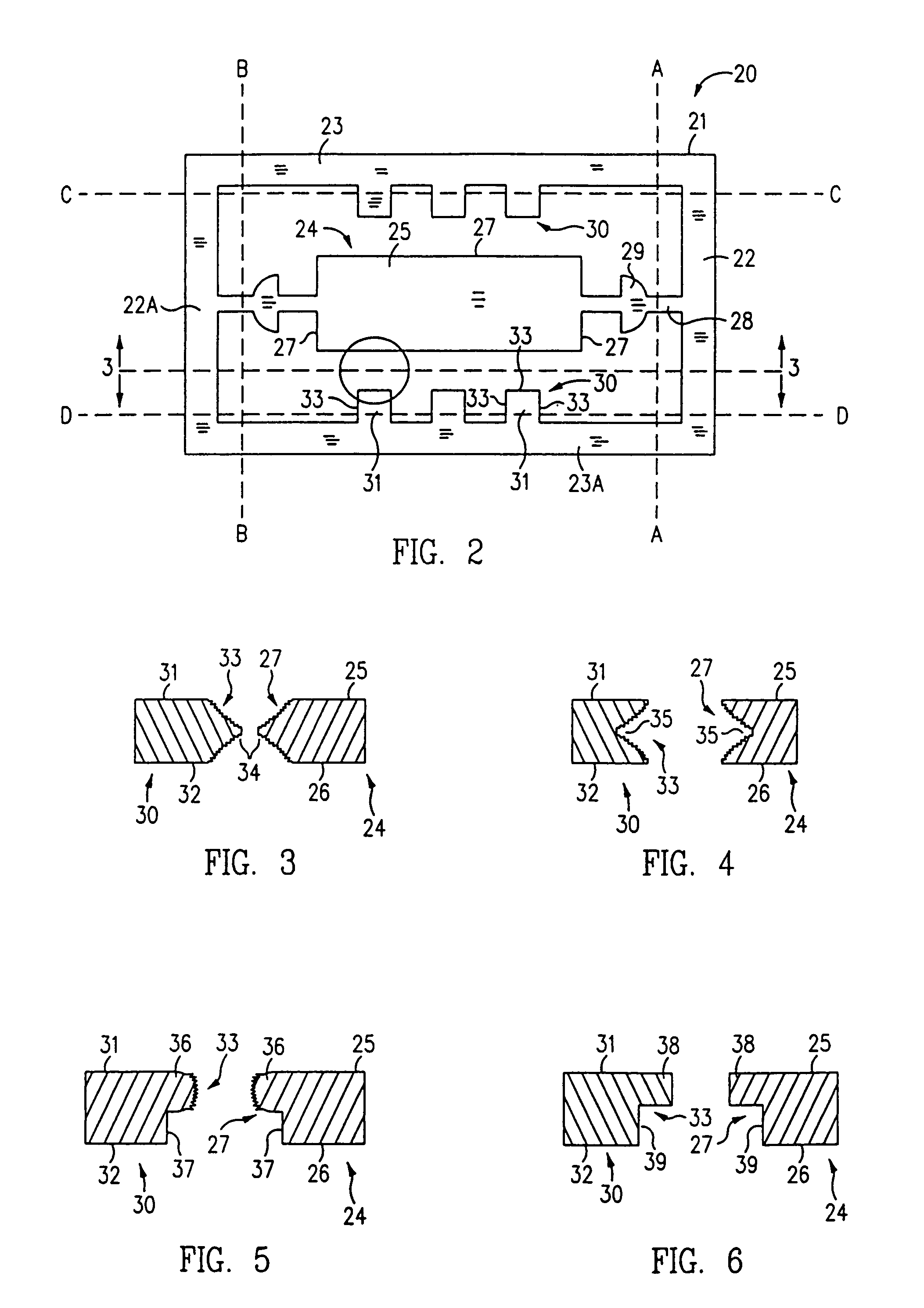
[0030]Step 1 of FIG. 1 provides a metal leadframe. FIG. 2 is a top view of a first embodiment of a metal leadframe 20 in accordance with the present invention. For ease of view, shading is used in FIG. 2 to distinguish the metal portions of leadframe 20 from empty spaces between the various elements of leadframe 20.

[0031]Leadframe 20 of FIG. 2 is planar or substantially planar and is made of a conventional leadframe metal, such as copper or copper alloys, plated copper or plated copper alloys, Alloy 42 (42% nickel, 58% iron), or copper plated steel, depending on the application. The opposing upper and lower surfaces of leadframe 20 may be plated with different metals. For example, the tabs 30 and / or other portions of leadframe 20 which ultimately are enclosed within the package may be plated with silver, gold, nickel palladium, or copper. Such pla...


PUM


Abstract

Packages for an integrated circuit die and methods and leadframes for making such packages are disclosed. The package includes a die, a die pad, peripheral metal contacts, bond wires, and an encapsulant. The die pad and contacts are located at a lower surface of the package. The die pad and the contacts have side surfaces which include reentrant portions and asperities to engage the encapsulant.A method of making a package includes providing a metal leadframe having a die pad in a rectangular frame. Tabs extend from the frame toward the die pad. The die pad and tabs have side surfaces with reentrant portions and asperities. A die is attached to the die pad. The die is electrically connected to the tabs. An encapsulant is applied to the upper and side surfaces of the leadframe. Finally, the leadframe is cut in situ so that the die pad and tabs are severed from the frame, the sides of the package are formed, and the package is severed from the leadframe.

Description

RELATED APPLICATIONS[0001]The present application is a continuation of U.S. application Ser. No. 10 / 688,710 entitled METHOD OF MAKING AN INTEGRATED CIRCUIT PACKAGE filed Oct. 17, 2003, which is a continuation of U.S. application Ser. No. 10 / 007,337 entitled METHOD OF MAKING AN INTEGRATED CIRCUIT PACKAGE filed Oct. 22, 2001 and issued as U.S. Pat. No. 6,684,496 on Feb. 3, 2004, which is a continuation of U.S. application Ser. No. 09 / 393,016 entitled PLASTIC INTEGRATED CIRCUIT PACKAGE AND METHOD AND LEADFRAME FOR MAKING THE PACKAGE filed Sep. 10, 1999 and now abandoned, which is a divisional of U.S. application Ser. No. 09 / 103,760 entitled PLASTIC INTEGRATED CIRCUIT CHIP PACKAGE AND METHOD AND LEADFRAME FOR MAKING THE PACKAGE filed Jun. 24, 1998 and issued as U.S. Pat. No. 6,143,981 on Nov. 7, 2000.FIELD OF THE INVENTION[0002]The present invention is to directed toward an improved plastic package for an integrated circuit die, and a method of making such a package.BACKGROUND OF THE IN...

Claims


Application Information

Patent Timeline
Patent Type & Authority Patents(United States)
IPC IPC(8): H01L21/50
CPCH01L23/49548H01L23/3107H01L2224/48091H01L2224/48247H01L2924/01046H01L24/48H01L2924/01079H01L2924/14H01L2924/15311H01L2924/01078H01L2924/00014H01L2924/181H01L2924/00012H01L2224/45099H01L2224/45015H01L2924/207
Inventor GLENN, THOMAS P.
Owner AMKOR TECH SINGAPORE HLDG PTE LTD
Why Eureka
Try Eureka