High speed differential signaling logic gate and applications thereof
What is Al technical title?
Al technical title is built by PatSnap Al team. It summarizes the technical point description of the patent document.
a logic gate and high-speed technology, applied in the field of signals processing, can solve the problems of increasing power consumption, reducing supply voltage for newer integrated circuit fabrication processes, and using traditional logic gates
Inactive Publication Date: 2006-02-14
AVAGO TECH WIRELESS IP SINGAPORE PTE
View PDF7 Cites 3 Cited by
Summary
Abstract
Description
Claims
Application Information
AI Technical Summary
This helps you quickly interpret patents by identifying the three key elements:
Problems solved by technology
Method used
Benefits of technology
[0012]The high-speed differential signaling logic gate of the present invention substantially meets these needs and others. In one embodiment of a high speed differential signaling logic gate, it includes a 1st input transistor, 2nd input transistor, complimentary transistor, current source, a 1st load, and a 2nd load. The 1st input transistor is operably coupled to receive a 1st input logic signal, which may be one phase of a first differential input signal. The 2nd input transistor is coupled in parallel with the 1st input transistor and is further coupled to receive a 2nd input logic signal, which may be one phase of a 2nd differential input signal. The complimentary transistor is operably coupled to the sources of the 1st and 2nd input transistors and to receive a complimentary input signal. The complimentary input signal mimics the other phase of the 1st differential logic signal and the 2nd differential logic signal.
Problems solved by technology
Issues arise with the use of traditional logic gates in applications that push the operating limits of an integrated circuit process.
For example, for a multi-gigahertz frequency range of operation, traditional logic gates create a bottleneck for the local oscillator due to the time it takes for each logic gate to complete its function.
Another related issue results as supply voltages decrease for newer integrated circuit fabrication processes (e.g., CMOS, gallium arsenide, silicon germanium, et cetera).
However, by increasing the supply voltage, power consumption increases, and, in many ways, defeats the benefit of newer integrated circuit fabrication processes.
As such, differential logic gates suffer from the above-mentioned issues as well.
Method used
Image
Click on the blue label to locate the original text in one second.
Reading with bidirectional positioning of images and text.
Examples
Embodiment Construction
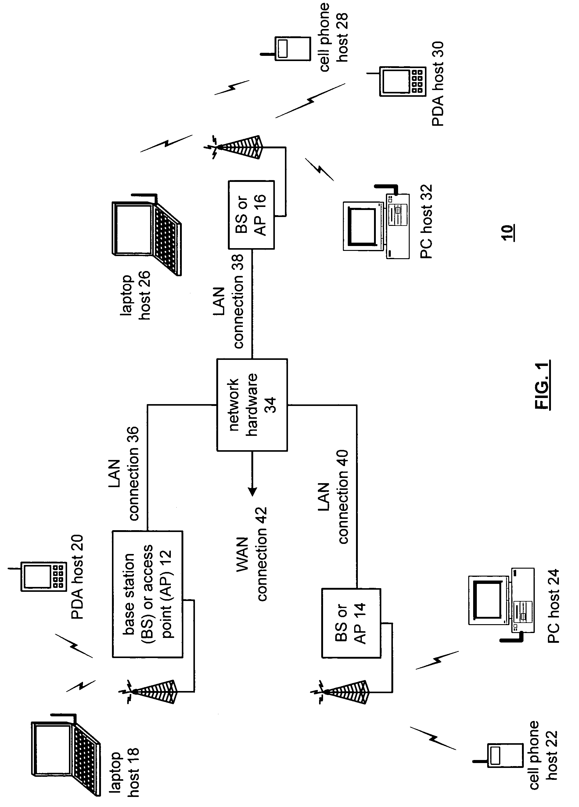
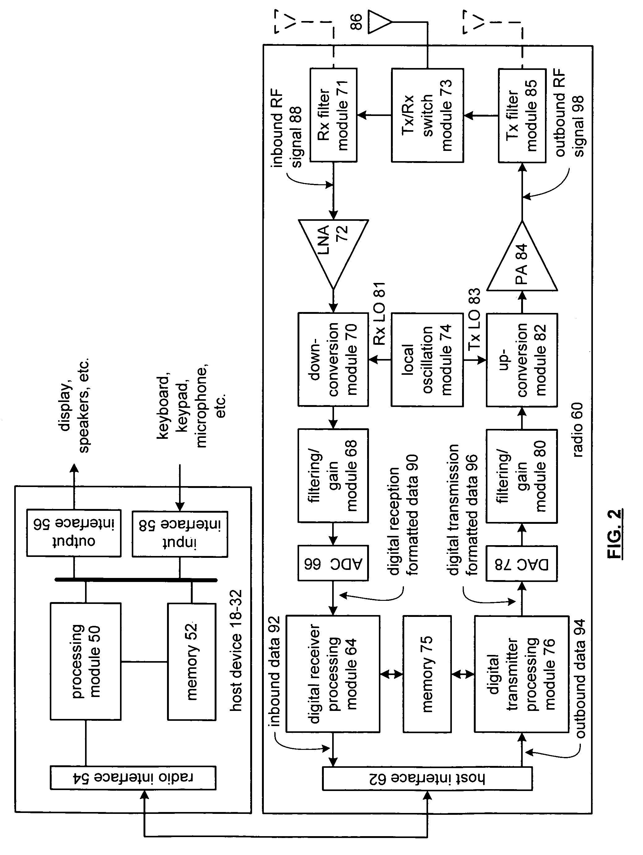
[0028]FIG. 1 is a schematic block diagram illustrating a communication system 10 that includes a plurality of base stations and / or access points 12–16, a plurality of wireless communication devices 18–32 and a network hardware component 34. The wireless communication devices 18–32 may be laptop host computers 18 and 26, personal digital assistant hosts 20 and 30, personal computer hosts 24 and 32 and / or cellular telephone hosts 22 and 28. The details of the wireless communication devices will be described in greater detail with reference to FIG. 2.
[0029]The base stations or access points 12–16 are operably coupled to the network hardware 34 via local area network connections 36, 38 and 40. The network hardware 34, which may be a router, switch, bridge, modem, system controller, et cetera provides a wide area network connection 42 for the communication system 10. Each of the base stations or access points 12–16 has an associated antenna or antenna array to communicate with the wirele...
PUM
Abstract
A high-speed differential signaling logic gate includes a 1st input transistor, 2nd input transistor, complimentary transistor, current source, a 1st load, and a 2nd load. The 1st input transistor is operably coupled to receive a 1st input logic signal, which may be one phase of a first differential input signal. The 2nd input transistor is coupled in parallel with the 1st input transistor and is further coupled to receive a 2nd input logic signal, which may be one phase of a 2nd differential input signal. The complimentary transistor is operably coupled to the sources of the 1st and 2nd input transistors and to receive a complimentary input signal, which mimics the other phase of the 1st differential logic signal and the 2nd differential logic signal. The current source sinks a fixed current from the 1st and 2nd input transistors and the complimentary transistor. The 1st load is operably coupled to the drains of the 1st and 2nd input transistors to provide a 1st phase of a differential logic output. The 2nd load is coupled to the drain of the complimentary transistor to provide a 2nd phase of the differential logic output.
Description
[0001]This patent application is claiming priority under 35 USC § 120 to patent application entitled HIGH SPEED DIFFERENTIAL SIGNALING LOGIC GATE AND APPLICATIONS THEREOF, having a Ser. No. 10 / 201,108, and a filing date of Jul. 23, 2002 now U.S. Pat. No. 6,756,821.BACKGROUND OF THE INVENTION[0002]1. Technical Field of the Invention[0003]This invention relates generally to signal processing and more particularly to logic gates.[0004]2. Description of Related Art[0005]Digital logic circuits such as AND gates, NAND gates, NOR gates, OR gates, exclusive OR gates, latches, inverters, flip-flops, et cetera are known to be used in a wide variety of electronic devices. For instance, digital logic circuits are used in all types of computers (e.g., laptops, personal computers, personal digital assistants, et cetera), entertainment equipment (e.g., receivers, televisions, et cetera), and wireless communication devices (e.g., cellular telephones, radios, wireless local area network devices, et ...
Claims
Application Information
Patent Timeline
Application Date:The date an application was filed.
Publication Date:The date a patent or application was officially published.
First Publication Date:The earliest publication date of a patent with the same application number.
Issue Date:Publication date of the patent grant document.
PCT Entry Date:The Entry date of PCT National Phase.
Estimated Expiry Date:The statutory expiry date of a patent right according to the Patent Law, and it is the longest term of protection that the patent right can achieve without the termination of the patent right due to other reasons(Term extension factor has been taken into account ).
Invalid Date:Actual expiry date is based on effective date or publication date of legal transaction data of invalid patent.