Structure for reducing the diffraction effect in periodic electrode arrangements and liquid crystal device including the same
a liquid crystal device and periodic electrode technology, applied in semiconductor devices, semiconductor/solid-state device details, instruments, etc., can solve the problems of incident light diffraction, narrow viewing angle, electrodes cannot be placed on one side of two substrates, etc., and achieve the effect of reducing the diffraction
- Summary
- Abstract
- Description
- Claims
- Application Information
AI Technical Summary
Benefits of technology
Problems solved by technology
Method used
Image
Examples
first embodiment
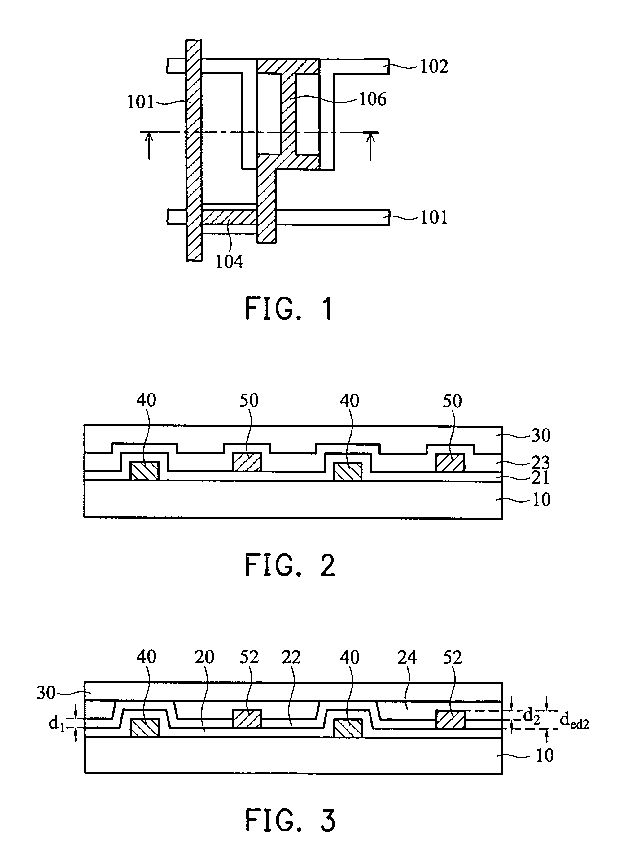
[0047]FIG. 2 is a cross section along the line II-II′ of the lower substrate in FIG. 1. The second electrode 0.50 is a transparent electrode, and the dielectric layer 23 is a transparent dielectric layer. Due to different optical paths of incident lights, light diffracts due to the diffraction effect in this periodic electrode arrangements.
[0048]The first embodiment is designed to reduce the diffraction effect for the structure described above.
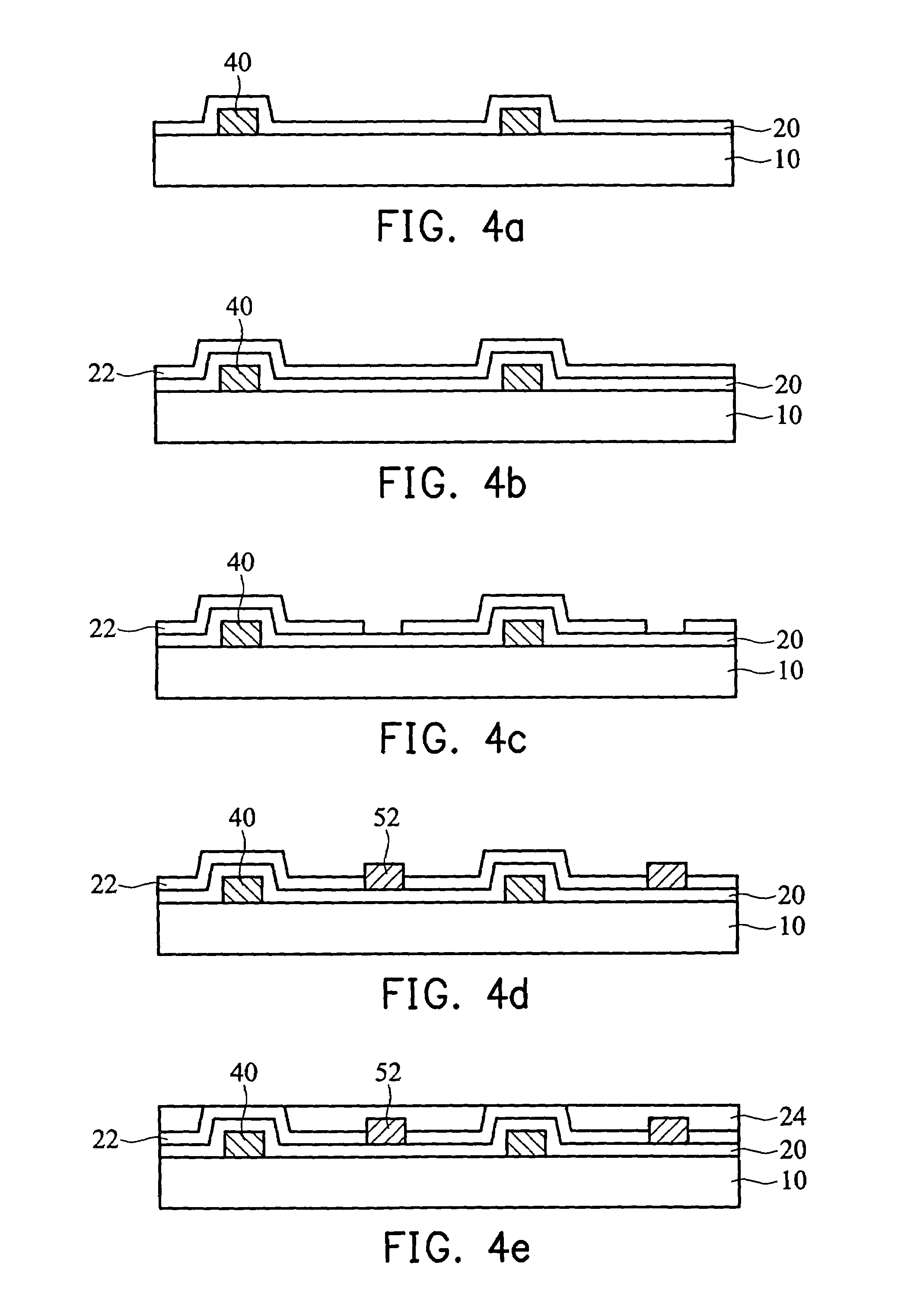
[0049]FIG. 3 is a cross section showing the lower substrate of the first embodiment of the invention. In FIG. 4a, a dielectric layer 10 having first electrodes 40 formed thereon is provided, and a first transparent dielectric layer 20 is formed to cover the first electrodes. A second transparent dielectric layer 22 having a predetermined thickness d1 is then formed on the first transparent dielectric layer 20, as shown in FIG. 4b.
[0050]Then, the second transparent dielectric layer 22 is etched using the first transparent dielectric layer 20 a...
second embodiment
[0054]FIG. 2 is cross section along the line II-II′ of the lower substrate in FIG. 1. The second electrode 40 is a transparent electrode, and the dielectric layers 21 and 23 are transparent dielectric layers. Due to different optical paths of incident lights, light diffracts due to the diffraction effect in this periodic electrode arrangements.
[0055]The second Embodiment is designed to solve the diffraction problem in the above structure. FIG. 5 is cross section showing the lower substrate of the second embodiment of the invention. A transparent dielectric layer 20 having a predetermined thickness d1 is formed on a dielectric layer 10, followed by etching the first transparent dielectric layer 20 to define the transparent electrode areas. Transparent electrodes 42 are then plated onto the transparent electrode areas.
[0056]The second transparent electrode 42 is then etched using the first transparent dielectric layer 20 as an etch stop layer, thus forming a transparent electrode 42 h...
third embodiment
[0060]FIG. 2 is cross section along the line II-II′ of the lower substrate in FIG. 1. The first electrode 40 and the second electrode 50 are transparent electrodes, and the dielectric layers 21 and 23 are transparent dielectric layers. Due to different optical paths of incident lights, light diffracts due to the diffraction effect in this periodic electrode arrangement.
[0061]The third embodiment is designed to reduce the diffraction effect in the above structure. FIG. 6 is cross section showing the lower substrate of the 3rd embodiment of the invention. A transparent dielectric layer 20 having a predetermined thickness d1 and a first transparent electrode 42 having a predetermined thickness ded1 are formed on a dielectric layer 10. A second transparent dielectric layer 22 having a predetermined thickness n2 is then formed on the first transparent dielectric layer 20 and the first transparent electrode 42.
[0062]The second transparent dielectric layer 22 is etched using the first tran...
PUM
| Property | Measurement | Unit |
|---|---|---|
| transparent | aaaaa | aaaaa |
| thicknesses | aaaaa | aaaaa |
| thickness | aaaaa | aaaaa |
Abstract
Description
Claims
Application Information
 - R&D
- Intellectual Property
- Life Sciences
- Materials
- Tech Scout
- Unparalleled Data Quality
- Higher Quality Content
- 60% Fewer Hallucinations
Browse by: Latest US Patents, China's latest patents, Technical Efficacy Thesaurus, Application Domain, Technology Topic, Popular Technical Reports.
© 2025 PatSnap. All rights reserved.Legal|Privacy policy|Modern Slavery Act Transparency Statement|Sitemap|About US| Contact US: help@patsnap.com


