Integrated mode converter and multiplexer

a converter and multiplexer technology, applied in the field of photonics, can solve the problems of significant performance degradation long propagation length, etc., and achieve the effects of low loss, high extinction ratio, and wide bandwidth

Active Publication Date: 2020-07-16
CONSEJO SUPERIOR DE INVESTIGACIONES CIENTIFICAS (CSIC) +1
View PDF0 Cites 6 Cited by
  • Summary
  • Abstract
  • Description
  • Claims
  • Application Information

AI Technical Summary

Benefits of technology

The patent describes a new device called a mode converter and multiplexer that has several technical benefits. First, it includes a subwavelength region made up of alternating sections of core and cladding materials that can suppress diffraction effects and enhance bandwidth. Second, the device has three preferred alternatives for phase-shifters that work synergistically with the MMI to provide better bandwidth, compact footprint, high extinction ratio, and high tolerance to fabrication deviations. Overall, the device has a very wide bandwidth with low losses and high extinction ratio in a compact design.

Problems solved by technology

However, ADC and RR are inherent narrowband devices, whereas other coupling-based solutions require long propagation lengths as they rely on mode-evolution.
Depending on their particular implementation, asymmetrical y-junctions either require long propagation lengths, or are very sensitive to fabrication deviations from the ideal design.
That is, a small variation in the fabricated waveguide width compared to its nominal value, inevitable when mass-producing the photonic interconnects, results in significant performance degradation.
Nevertheless, MMI-based solutions are limited by the MMI excess losses and dispersion profile, ultimately limiting bandwidth improvement.

Method used

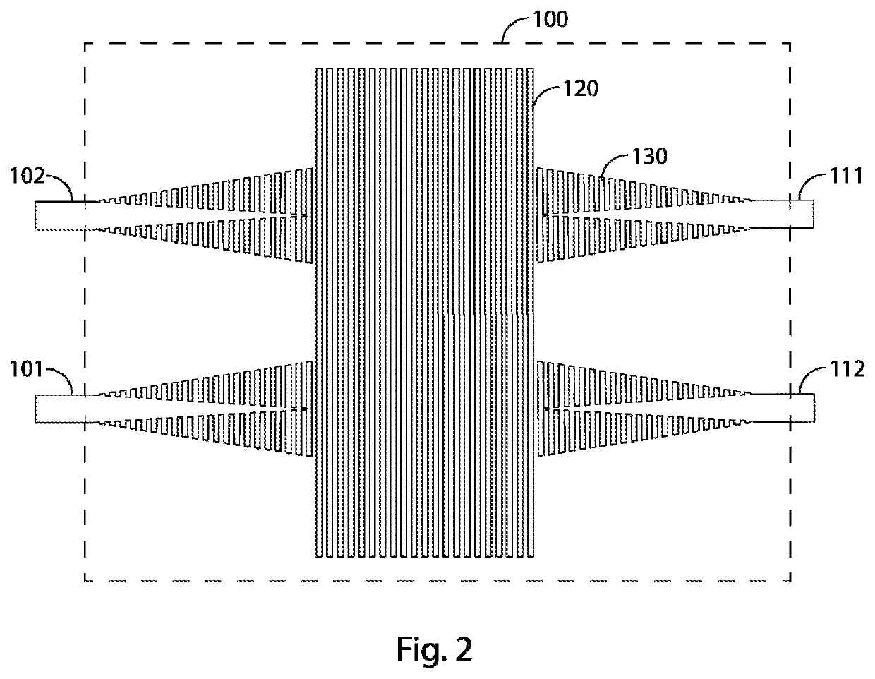
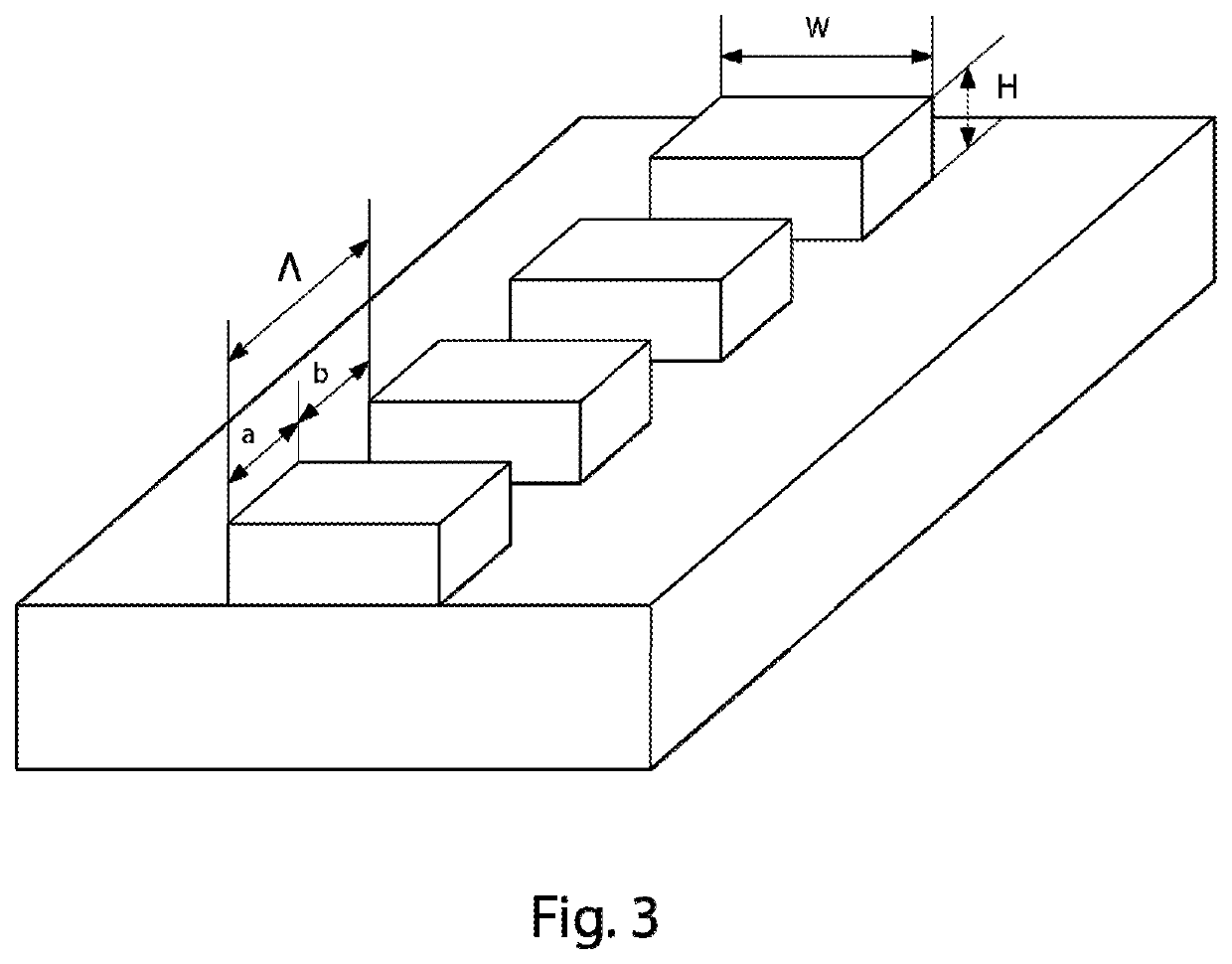

Image

  • Integrated mode converter and multiplexer
  • Integrated mode converter and multiplexer
  • Integrated mode converter and multiplexer

Examples


first embodiment

[0043]FIG. 4 presents the phase-shifter (200), comprising a first waveguide (201) and a second waveguide (202). The second waveguide (202) is a conventional wire waveguide with a first width (w1) without any geometrical modifications, whereas the first waveguide starts with the first width (w1), but comprise two symmetrical trapezoidal regions (210, 211) which widen the waveguide up to a second width (w2) and then decrease back to the first width (w1). As a consequence, mode velocity is reduced and the desired phase shift is induced. Notice that alternative embodiments based on the same principle may be implemented, for example substituting the trapezoidal regions (210, 211) for other width profiles, such as curves; by adding a central region with constant second width (w2) between the trapezoidal regions (210, 211); by using a second width (w2) smaller than the first width (w1), and / or by any other combination of width variations resulting in the same total phase-shift.

[0044]In ord...

third embodiment

[0048]FIG. 6, presents the phase-shifter of the invention, relying on one or more phase-loading segments (250) at the sides of the first waveguide (201). Said first waveguide (201) preferably presents a reduced width (w5) in the region where the phase-loading segments (250) are located to delocalize the optical mode and enhance the effect of said segments. Width reduction is preferably performed progressively through mode adapters. Furthermore, the phase loading segments (250) may comprise additional geometrical features on their extremes to obtain a smoother effective index transition, such as angled, curved or thinned extremes.

[0049]Similar width reductions as in the first waveguide (201) may be also implemented in the second waveguide (202), down to the same reduced width (w5) or to a different width, to optimize bandwidth. Furthermore, said second waveguide (202) may also comprise phase-loading segments (250), as long as they present different geometrical properties. Also, the p...


PUM


Abstract

An integrated mode converter and multiplexer ( / demultiplexer) is disclosed, which combines a multimode interference coupler (100), at least one phase-shifter (200) and a symmetrical Y-junction (300). The dispersion of the multimode interference coupler (100) is engineered through subwavelength structures in order to achieve a very wide bandwidth. Several phase-shifter (200) topologies for further bandwidth enhancement are disclosed, as well as architectures for multiplexing a greater number of optical modes.

Description

FIELD OF THE INVENTION[0001]The present invention has its application within the photonics sector and, especially, in the industrial area engaged in providing waveguide-based mode converter and multiplexers.BACKGROUND OF THE INVENTIONRelated Art[0002]High-capacity photonic interconnects are highly sought-after in order to exceed the capacity limits imposed by traditional copper interconnects. Some advantages of photonic interconnects are lower power consumption, circumvention of parasitic capacitance and compatibility with a plurality of multiplexing techniques to increase the overall aggregated bandwidth. For example, wavelength division multiplexing (WDM), polarization division multiplexing (PDM) and space division multiplexing (SDM) schemes can be combined to scale up the data-transmission capacity of the devices, in an attempt to cover the steadily growing demand of new services handling data volumes.[0003]All these techniques can be combined with mode division multiplexing (MDM...

Claims


Application Information

Patent Timeline
Patent Type & Authority Applications(United States)
IPC IPC(8): G02B6/12G02B6/14G02B6/28G02B6/125
CPCG02B2006/12164G02B2006/12088G02B6/14G02B2006/1209G02B2006/12152G02B6/125G02B6/2813G02B6/12007G02B6/12004G02B6/1228G02B6/124G02F1/217G02B6/34G02F1/011G02F1/225
Inventor GONZÁLEZ ANDRADE, DAVIDVILLAFRANCA VELASCO, AITORCORREDERA GUILÉN, PEDROWANGÜEMERT PÉREZ, J. GONZALOORTEGA MOÑUX, ALEJANDROHALIR, ROBERTMOLINA FERNÁNDEZ, IÑIGO
Owner CONSEJO SUPERIOR DE INVESTIGACIONES CIENTIFICAS (CSIC)
Why Eureka
Try Eureka