Method of forming semiconductor device by crystallizing amorphous silicon and forming crystallization promoting material in the same chamber
a technology of crystallization promotion and semiconductor devices, which is applied in the direction of semiconductor devices, basic electric elements, electrical appliances, etc., can solve the problems of difficult to use an inexpensive glass substrate as a substrate, low electrical characteristic and limited use of amorphous silicon films
- Summary
- Abstract
- Description
- Claims
- Application Information
AI Technical Summary
Benefits of technology
Problems solved by technology
Method used
Image

Examples
embodiment 1
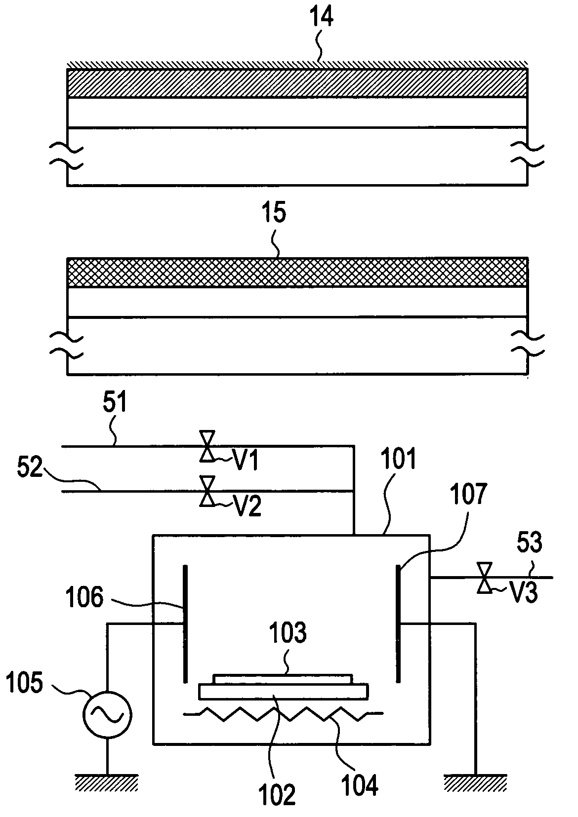
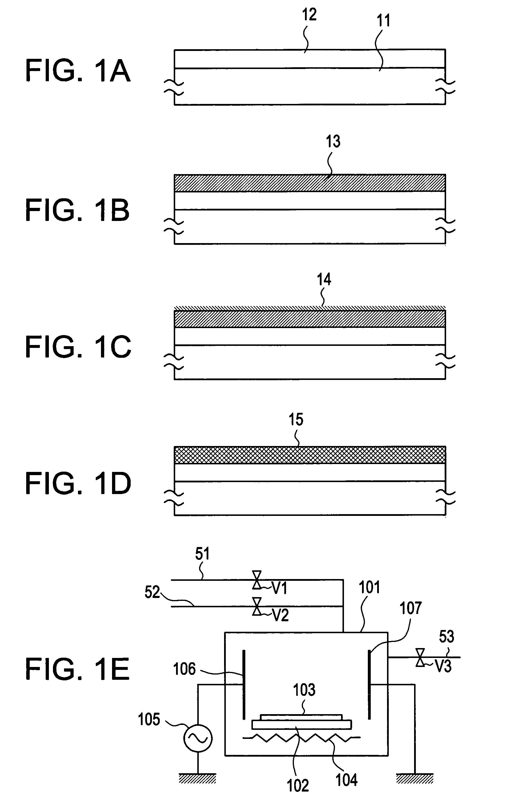
[0038]The embodiment shows a method for forming a silicon film having crystalline on a glass substrate. Referring to FIGS. 1A to 1E, a process will be described until introduction of a catalytic element (nickel in the embodiment) and crystallization. A substrate is a Corning 7059 glass having a size of 100 mm×100 mm.
[0039]A silicon oxide film 12 having a thickness of 1000 to 5000 Å, for example, 2000 Å, is formed on a substrate 11 by sputtering and plasma chemical vapor deposition (plasma CVD). (FIG. 1A)
[0040]An amorphous silicon film 13 having a thickness of 100 to 1500 Å is formed by plasma CVD and low pressure CVD (LPCVD). In the embodiment, the amorphous silicon film 13 having a thickness of 500 Å is formed by plasma CVD. (FIG. 1B)
[0041]Fluorinating is performed to remove dirt and a natural oxide film, and then the substrate 11 is placed in a chamber 101 as shown in FIG. 1E. An introducing tube for introducing a gas from an external and an exhaust tube 53 are connected to the ch...
embodiment 2
[0054]In the embodiment, an apparatus as similar to EMBODIMENT 1 is used, and an organic nickel is decomposed by plasma instead of heat. Referring to FIGS. 1A to 1E, a process will be described until introduction of a catalytic element (nickel in the embodiment) and crystallization. A substrate is a Corning 7059 glass having a size of 100 mm×100 mm.
[0055]A process is performed as similar to EMBODIMENT 1 until the amorphous silicon film 13 formed on the substrate 11 is placed in the chamber 101 after a natural oxide film is removed.
[0056]After the substrate 11 is placed in the chamber 101, an organic nickel is introduced as similar to EMBODIMENT 1. Since the object of the embodiment is to decompose an organic nickel by using plasma, it is necessary to set a low pressure in the chamber 101. It is desired that the pressure is about 1 to 1000 Pa. In the embodiment, the pressure is adjusted to 20 Pa.
[0057]As described above, in EMBODIMENT 1, the parallel plate type electrodes 106 and 107...
embodiment 3
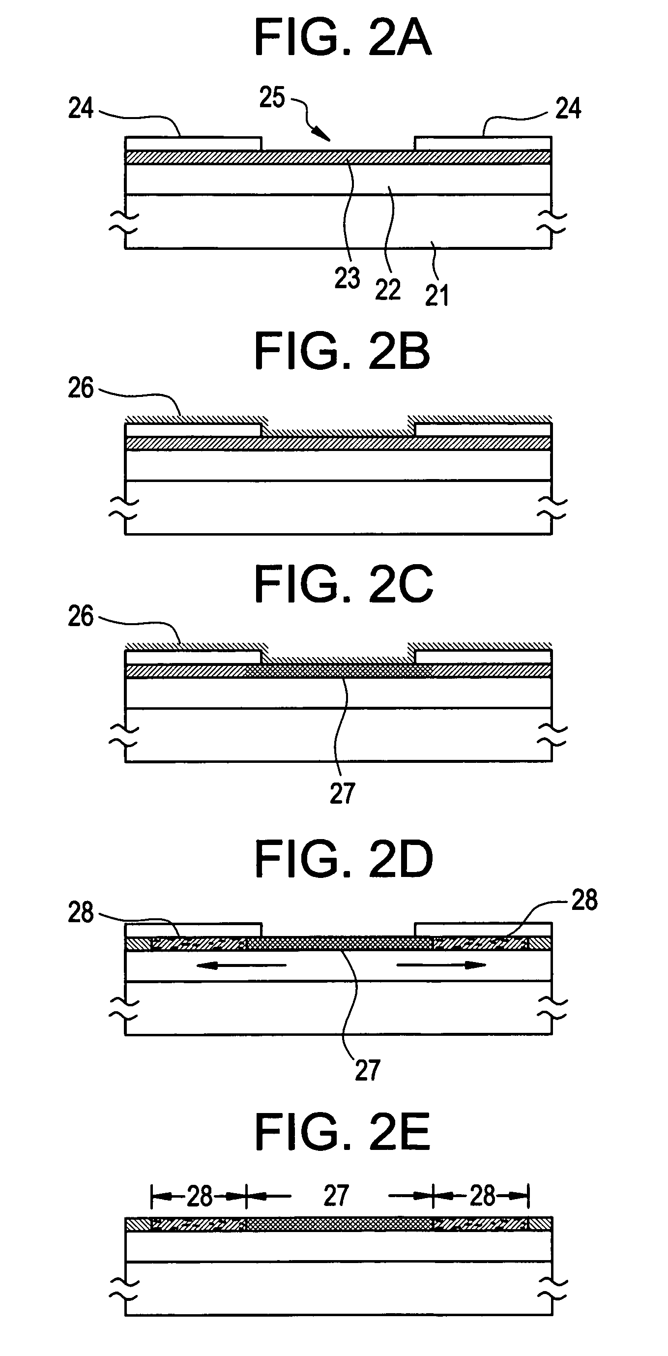
[0064]In the embodiment, after a nickel film is formed on a surface of an amorphous silicon film by a method as shown in EMBODIMENT 2, a nickel silicide is formed on the surface and then thermal crystallization is performed. A process until an organic nickel is decomposed and deposited by RF plasma is performed as similar to EMBODIMENT 2.
[0065]To exhaust (remove) a remaining gas from the chamber, the valve V3 is opened, so that an organic nickel is exhausted completely. After that, only carrier gas is introduced by opening V2. A pressure is desired to be about 1 to 1000 Pa which is almost equal to a pressure when the organic nickel is decomposed. In the embodiment, the pressure is 25 Pa.
[0066]In the chamber including only carrier gas, an RF energy is applied to the electrodes 106 and 106 to produce plasma. By processing an amorphous silicon film on which a nickel film is deposited, using the plasma, a nickel silicide is formed by nickel and amorphous silicon. This is due to an energ...
PUM
 Abstract
Description
Claims
Application Information
 - R&D
- Intellectual Property
- Life Sciences
- Materials
- Tech Scout
- Unparalleled Data Quality
- Higher Quality Content
- 60% Fewer Hallucinations
Browse by: Latest US Patents, China's latest patents, Technical Efficacy Thesaurus, Application Domain, Technology Topic, Popular Technical Reports.
© 2025 PatSnap. All rights reserved.Legal|Privacy policy|Modern Slavery Act Transparency Statement|Sitemap|About US| Contact US: help@patsnap.com