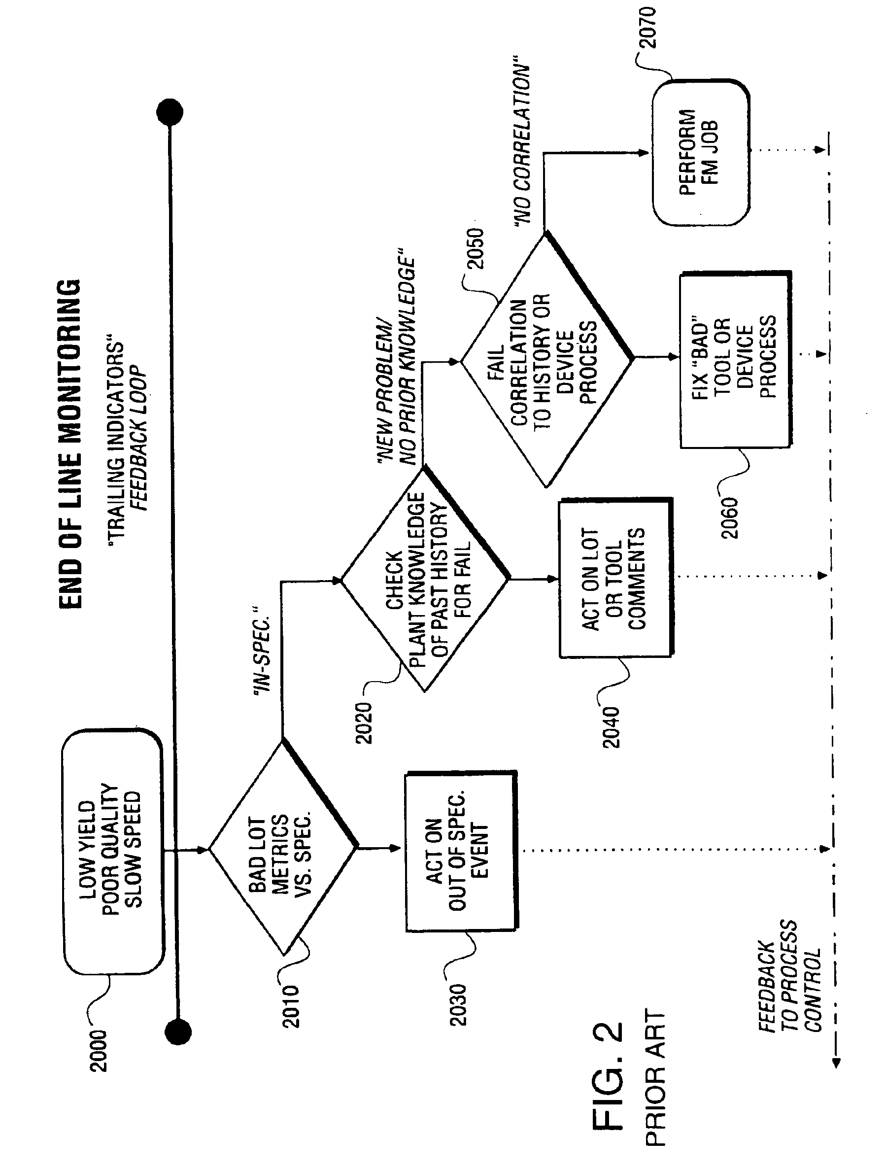
There are several problems associated with the above-described end-of-line monitoring process.
For example: (a) low yield is often produced by several problems; (b) “spec” limits are often set as a result of unconfirmed theories; (c) knowledge of past product failure history is often not documented or, if it is documented, the
documentation is not widely distributed; (d) data and
data access is fragmented; and (e) a working
hypothesis must be generated prior to performing a
correlation analysis, the number of correlations is very large, and resources used to perform the
correlation analysis is limited.
These issues are made no easier by a transition to 300 mm wafers.
Thus, with many things converging simultaneously, yield ramping is becoming a major hurdle.
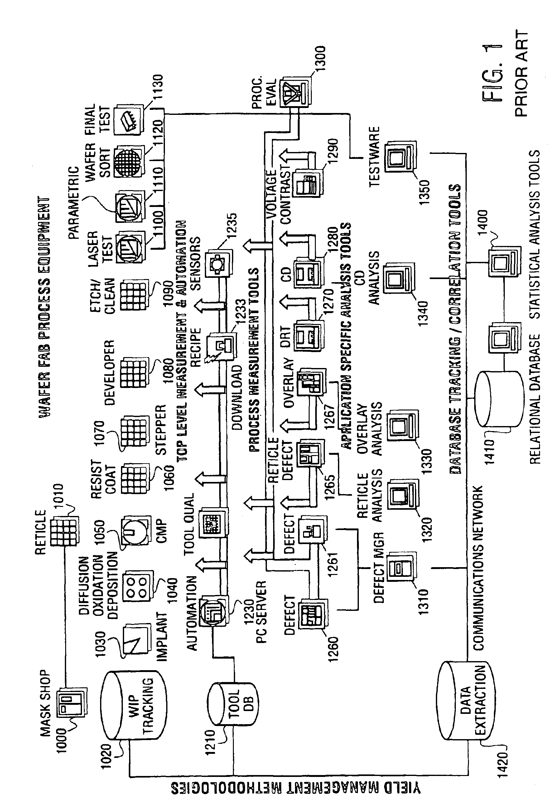
In addition to the above-identified problems, a further problem arises in that
semiconductor fabs spend a large amount of their capital on defect detection equipment and defect
data management software in an effort to monitor defectivity, and continuously reduce defect densities.
For each of these deliverables, a main drawback is that a user has to have prior knowledge of what he / she wants to plot.
However, due to the magnitude of the data, the probability of the user trending a
root cause is low.
Moreover, even if charts were generated for every variable, given the large number of charts, it would be virtually impossible for the user to analyze every one of such charts.
In addition to the above-identified problems, a further problem arises in that much of the data utilized in the
semiconductor fab is “indirect
metrology data.” The term “indirect
metrology” in this context indicates data gathering on indirect
metrics, which indirect
metrics are assumed to relate in predictable ways to manufacturing process within the fab.
However, in practice, indirect
metrology identifies a large number of potential issues, and these issues often lack a clear relationship to specific or “actionable” fab
processing tools or
processing tool
processing conditions.
This lack of a clear relationship between the processing toolset and much of a
semiconductor fab's indirect metrology results in a significant investment in
engineering staffing infrastructure, and a significant “
scrap” material cost due to the unpredictable timeframe required to establish causal relationships within the data.
Although temporal based, process tool data is now available for some fraction of processing tools in at least some fabs, use of the data to optimize processing tool performance relative to the ICs being produced has been limited.
The difficulty associated with “merging” processing tool temporal data and discrete data
metrics has resulted in limited use of processing tool temporal data as a means to optimize factory efficiency.
In addition to the above-identified problems, a further problem arises that involves the use of relational databases to store the data generated in a fab.
In this regard, prior art relational databases have two inherent issues that cause problems when such relational databases are used in a fab.
The first issue is that a user (for example, aprogrammer) must have an intimate knowledge of the data prior to creating specific schema (i.e., relationships and
database tables) for the data to be modeled.
The second issue is that, although relational databases have excellent TPS ratings (i.e.,
transaction processing specifications) for retrieving
small data transactions (such as, for example, banking, airline ticketing, and so forth), they perform inadequately in generating large data sets in support of decision support systems such as data warehousing, and data mining required for, among other things, yield improvement in a fab.
In addition to the above-identified problems, a further problem arises as a result of prior art
data analysis algorithms that are used in the semiconductor manufacturing industry to quantify production yield issues.
These algorithms suffer from two basic problems: (a) there is almost always more than one yield impacting issue within a given set of data; however, these algorithms are best used to find “an” answer rather than quantify a suite of separate yield impacting issues within a given fab; and (b) these algorithms are not able to be completely automated for “hands off” analyses; i.e.,
linear regression analysis requires manual preparation and definition of variable categories prior to analysis, and the
decision tree data mining requires a “human user” to define a targeted variable within the analysis as well as to define various parameters for the analysis itself.
In addition to the above-identified problems, a further problem arises in data mining significantly large data sets.
Burdening these industry experts with the required data mining and correlation tasks introduces inefficiencies in use of their time, as well as inconsistencies in results obtained from process to process, since the process of data mining is largely driven by manual intervention.
Ultimately, even when successful, much of the “gains” have been lost or diminished.
For example, the
time consuming process of manually manipulating the data and analysis is costly, in man hours and equipment, and if the results are not achieved early enough, there is not enough time to implement discovered changes.
In addition to the above-identified problems, a further problem arises in as follows.
Given the vast number of tools and “tool-like” categorical data within
semiconductor fab databases, it is difficult to isolate a rogue processing tool using manual spreadsheet searching techniques (referred to as “commonality studies).
However, this technique requires prior knowledge of a specific process layer, and it can be
time consuming if a user does not have a good understanding of the nature of the failure.
These techniques can be effective, but extensive domain expertise required in data mining makes them difficult to set up.
In addition, these data mining algorithms are known to be slow due to the large amount of
algorithm overhead required with such generic
data analysis techniques.
Lastly, in addition to the above-identified problems, a further problem arises as follows.
However, when utilizing these algorithms to analyze large data sets on low cost hardware platforms such as Window 2000 servers, several limitations occur.
Of primary concern among these limitations is the utilization of
random access memory and extended CPU loading required by these techniques.
Often, a
neural network analysis of a large semiconductor manufacturing dataset (for example, >40 Mbytes) will persist over several hours, and may even breach the 2 Gbyte RAM limit for the Windows 2000
operating system.
