
Method for reducing wiring congestion in a VLSI chip design

a technology of integrated circuits and chip designs, applied in computer aided design, basic electric elements, instruments, etc., can solve the problems of inability to perform the desired function, and inability to guarantee the box's function, so as to avoid the congestion of wiring areas and never degrade the effect of congestion

Inactive Publication Date: 2005-10-25
IBM CORP
View PDF2 Cites 8 Cited by
  • Summary
  • Abstract
  • Description
  • Claims
  • Application Information

AI Technical Summary

Benefits of technology

The present invention provides a system and method for alleviating wiring congestion in a chip design. The invention uses global routing to restructure logic in ways that improve congested wiring areas without affecting other design attributes. The invention also includes identifying congested areas, optimizing wiring to improve congestion, and rerouting affected nets. The invention can reduce wiring pressure on specific grid edges and improve overall congestion in a chip design.

Problems solved by technology

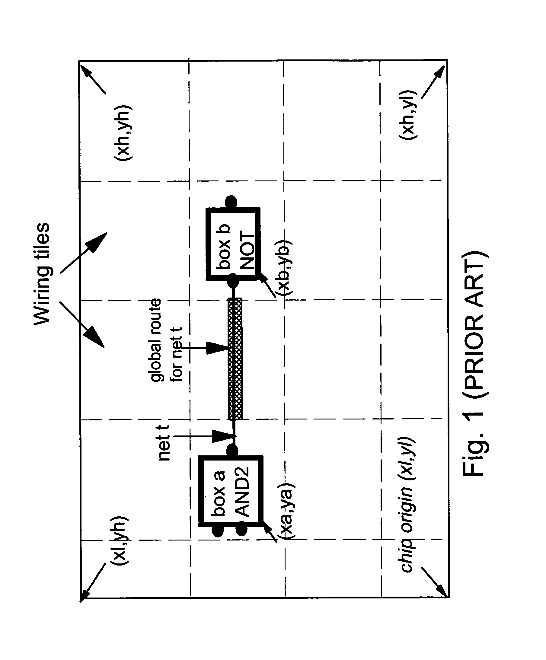
In general, placement follows some model of how this routing is to be accomplished, but the model is not exact and does not always predict the actual routes.
Placement is therefore unable to guarantee that the boxes will be placed in a manner such that all of the wires will be routed.
In addition, some boxes may represent functions requiring a large number of inputs / outputs, which may preclude placing them in a way that encourages ratability, unless the design is very sparse.
When all the wires cannot be routed, the chip will not perform the desired function and, thus, will not be manufacturable.
This is a time consuming and expensive process, since in today's large chips it is not unusual to find thousands of wires that cannot be routed.
In addition, in the event that an error is found in the logical design, this fix-up step may need to be repeated several times.
Wiring congestion occurs when the number of wire passing through an area of the circuit design exceeds the space available for wiring.
As previously mentioned, when wiring congestion occurs, the design cannot be manufactured.
Additional constraints include electrical constraints, which limit the amount of capacitance on any net and the maximum amount of slew time that can be tolerated.
In some cases, more elaborate methods of congestion prediction are used, but no known method guarantees that the outcome of the placement will always be routed without congestion.
Given a global route, it is not always possible to achieve a detailed route because the routes cannot be completed from the grid edge to the pins.
While this alleviates certain congestion problems, the simultaneous placement and routing systems do not guarantee uncongested designs and provide no recourse when global congestion occurs.
These methods are not guaranteed to improve congestion.
Since they work with estimates that often do not reflect the actual wire routes, they may optimize the wrong areas and, sometimes, increase wiring congestion.
A weakness of both of the above restructuring methods is that they improve wiring in the region selected, but have no affect on global wires because they do not take into consideration the effect of feedthrough wires.
Since these wires do not appear within the original region to be restructured, this kind of restructuring will not find solutions of the kind described in (a) and (b).
The aforementioned methods do not guarantee an improvement of the wireability of a design because global congestion is a function of placement, of the logic structure of the design and of the quality of the router.
It is possible that a design placement and logic structure will preclude a successful routing, but this cannot be determined until the routing is actually completed.
Estimates (e.g., rectilinear Steiner routes) do not provide sufficient detail and / or correlation with true routes to accurately predict congestion prior to the actual routing.
Furthermore, none of the above restructuring methods address the problems of relieving wiring congestion in the presence of other design constraints.
Even if the restructuring methods succeed in reducing congestion, it is achieved at the expense of adding timing, electrical, or power violations.
Correcting these violations entails modifying the size or structure of the logic or adding new logic elements, all of which must be replaced and rerouted, often causing new congestion problems.
Such methods are effective in improving the detailed wiring, but they do not address global congestion issues.

Method used


Image

  • Method for reducing wiring congestion in a VLSI chip design
  • Method for reducing wiring congestion in a VLSI chip design
  • Method for reducing wiring congestion in a VLSI chip design

Examples


Embodiment Construction

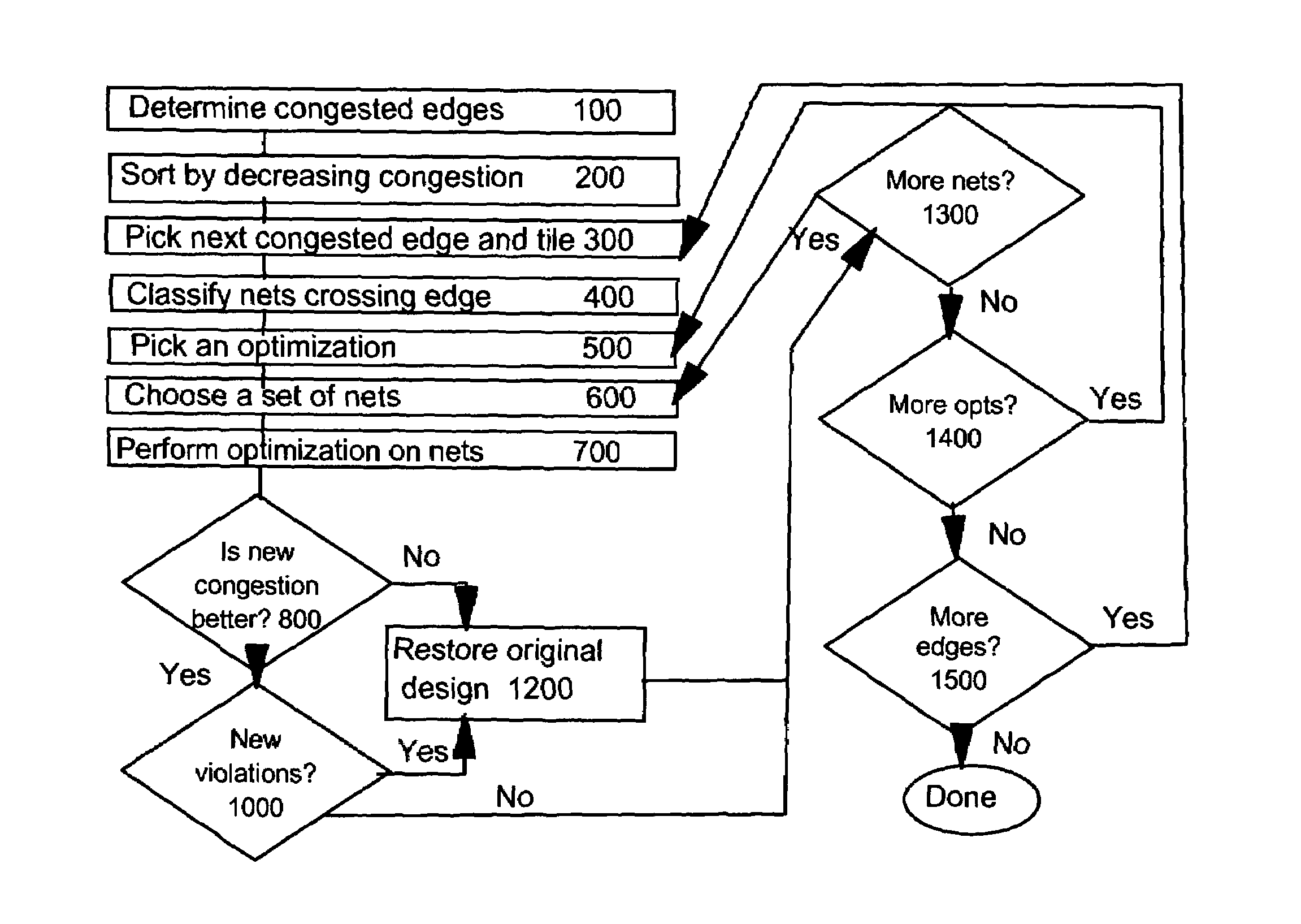
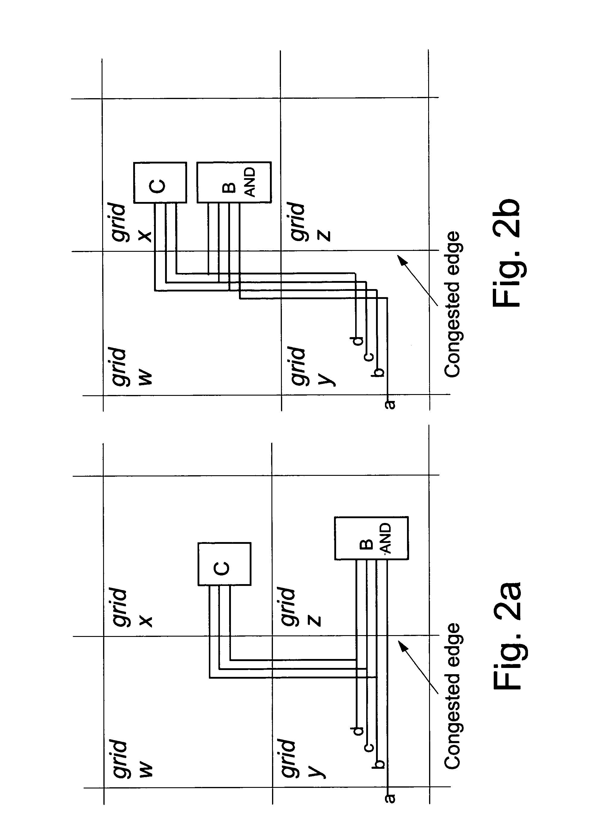
[0043]The novelty of the invention being described herein resides in applying transformations that move, decompose, add logic elements or modify wire connections in order to reduce congestion and provide a routable design. Hereinafter, an algorithm is provided along with incremental placement and incremental routing to relieve the wiring congestion. Success at this process reduces or eliminates the need for manual intervention on the part of the designer.

[0044]The method assumes that the design is already placed, optimized and globally routed. Global routing places a wiring grid over the design, as described above. Each edge of the grid has a known capacity which is the amount of wire Ci that can pass over edge I, and a utilization Ui, (i.e., how many wires cross the edge i, weighted by width), such that

Ui=Sum wire j crossing edge i widthj,  (Eq. 1)

wherein widthj is the width of wire j crossing edge i. (In the present example, for clarity sake, all the wires are assumed to have a wi...


PUM


Abstract

A system and method for correcting wiring congestion in a placed and partially or fully globally-routed VLSI chip design while avoiding adding new timing or electrical violations or other design constraints. Globally-congested areas are identified along with determining terminated and non-terminated wires in the congested areas. The process includes optimizing the identified congestion areas, incrementally rerouting affected nets, testing the resultant design legality and congestion metrics, and committing or reversing the optimizations and reroutings. The optimizations further includes the movement of logic cells and decomposition, recomposition or any other modification of logic cell structures (possibly combined with cell movement) to move terminated wires to less congested grid edges, rearrangement of commutative connections within or between cells, or addition of buffers to cause reroutes of feedthrough wires.

Description

FIELD OF THE INVENTION[0001]The present invention generally relates to very large scale integrated (VLSI) circuit design, and more particularly, to a system and method for restructuring logic to correct wiring congestion in a placed and partially or fully globally routed design to avoid adding new violations of other design constraints.BACKGROUND OF THE INVENTION[0002]In the production of standard-cell integrated-circuit chips, a designer first attempts to obtain a logical representation of the function the chip is to perform. The end result of the logic design is a netlist providing the necessary interconnections to boxes representing logic elements selected from a library. Upon completion of the logic design, a physical design must then be performed to translate the abstract logic design into its physical realization on the chip. The first step in the physical design process consists of placing boxes, wherein physical realizations of the library cells are used to place the boxes o...

Claims


Application Information

Patent Timeline
Patent Type & Authority Patents(United States)
IPC IPC(8): H01L29/40H01L23/52G06F17/50
CPCG06F17/5077G06F30/394
Inventor KOTECHA, POOJA M.GANDHAM, RAMA GOPALPURI, RUCHIRTREVILLYAN, LOUISE H.MATHENY, ADAM P.
Owner IBM CORP
Learn More