Flat panel display device and method of manufacturing the same

a technology of flat panel display and manufacturing method, which is applied in the direction of solid-state devices, electric lighting sources, and electroluminescent light sources, can solve the problems of low manufacturing yield and high production cost, and achieve the effect of reducing mask process and high manufacturing yield

Inactive Publication Date: 2005-10-25
SAMSUNG DISPLAY CO LTD
View PDF9 Cites 24 Cited by
  • Summary
  • Abstract
  • Description
  • Claims
  • Application Information

AI Technical Summary

Benefits of technology

The present invention provides an organic EL display with a high manufacturing yield by reducing mask processes. It also has excellent electrical characteristics and high light transmittance. The invention provides a flat panel display with contact holes, source and drain electrodes, and a third insulating layer. The method of manufacturing the display involves forming a pixel electrode and semiconductor layer on an insulating substrate, adding a first insulating layer to cover the electrodes, adding a gate electrode, adding a second insulating layer to cover the gate electrode, adding source and drain electrodes connected to the semiconductor layer and pixel electrode, adding a photoresist layer, and etching the insulating layers using the photoresist layer as a mask.

Problems solved by technology

Since seven complicated mask processes are used to manufacture the organic EL display, production cost is high and manufacturing yield is low.

Method used


Image

  • Flat panel display device and method of manufacturing the same
  • Flat panel display device and method of manufacturing the same
  • Flat panel display device and method of manufacturing the same

Examples


Embodiment Construction

[0034]Reference will now be made in detail to preferred embodiments of the present invention, examples of which are illustrated in the accompanying drawings, wherein like reference numerals refer to the like elements throughout. The embodiments are described below in order to explain the present invention by referring to the figures.

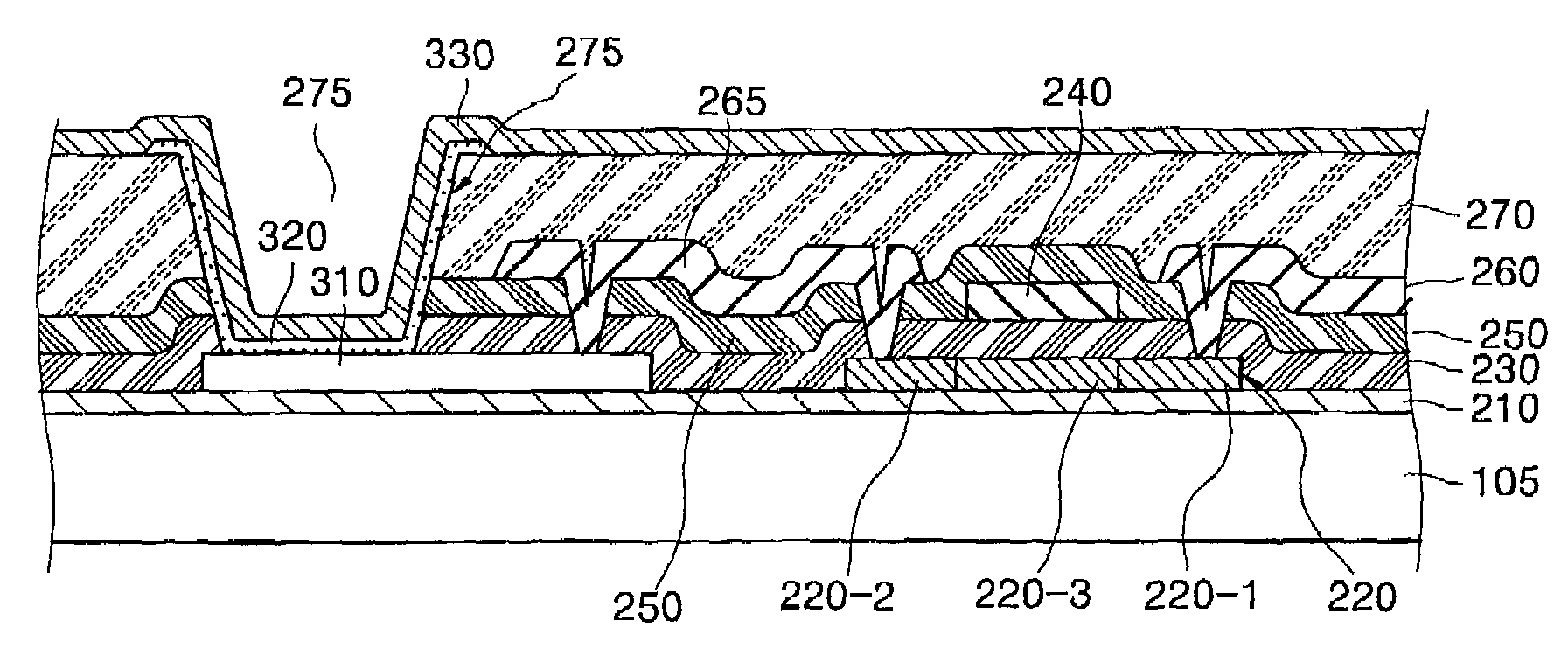
[0035]FIG. 2 shows a plan view illustrating an organic EL display 100 according to an embodiment of the present invention. Referring to FIG. 2, the organic EL display 100 includes pixels 130, where each pixel 130 includes first and second TFTs 110 and 200, a storage capacitor 170, and an organic EL element 300.

[0036]The pixel 130 is formed at a region defined by two adjacent gate lines 101, a data line 102 and a power supplying line 103. The gate lines 101 are arranged in a transverse direction. The data line 102 and the power supplying line 103 are arranged in a perpendicular direction to the gate lines 101. The gate lines 101 serve to apply a thin film...


PUM


Abstract

A flat panel display includes a pixel electrode having an opening portion formed on an insulating substrate, a semiconductor layer formed over a surface of the insulating substrate, spaced apart from the pixel electrode, having source and drain regions formed to both end portions thereof, a first insulating layer formed over the surface of the insulating substrate excluding the opening portion of the pixel electrode, a gate electrode formed on the first insulating layer over the semiconductor layer, and a second insulating layer formed over the surface of the insulating substrate excluding the opening portion of the pixel electrode. The present invention provides an organic EL display manufactured with reduced mask processes which has excellent electrical characteristics and improved light transmittance.

Description

CROSS-REFERENCE TO RELATED APPLICATIONS[0001]This application claims the benefit of Korean Patent Application No. 2001-19915, filed on Apr. 13, 2001, in the Korean Industrial Property Office, the disclosure of which is incorporated herein by reference.BACKGROUND OF THE INVENTION[0002]1. Field of the Invention[0003]The present invention relates to a flat panel display and a method of manufacturing the same. More particularly, the present invention relates to an organic electroluminescence (EL) display and a method of manufacturing the same.[0004]2. Description of the Related Art[0005]Electroluminescence (EL) displays have recently attracted considerable attention as a flat panel display. The EL displays generally use a thin film transistor (TFT) as a switching element.[0006]FIG. 1 is a cross-sectional view illustrating a conventional EL display. The conventional EL display of FIG. 1 is manufactured as follows. First, a first insulating layer 11 is formed on the whole surface of a tra...

Claims


Application Information

Patent Timeline
Patent Type & Authority Patents(United States)
IPC IPC(8): H01L21/70H01L27/12H01L21/84H05B33/10H01L21/77H01L27/32
CPCH01L27/1214H01L27/3244H01L27/3248H01L27/1288H01L27/3246H01L51/56H10K59/123H10K59/122H05B33/10H10K59/12H10K71/00
Inventor KIM, KEUM-NAM
Owner SAMSUNG DISPLAY CO LTD
Why Eureka
Try Eureka