
Integrated circuit cells

a technology of integrated circuits and cells, applied in the field of integrated circuit cells, can solve the problems of degrading the cell performance, unable to benefit from the selective use of low power cells, and inability to combine low power cells with high performance cells in certain ics, etc., to achieve simplified design and manufacturing processes, reduce the power consumption level of integrated circuits, and simplify the process of switching from high performance to low power cells.

Inactive Publication Date: 2005-10-11
TEXAS INSTR INC
View PDF2 Cites 223 Cited by
  • Summary
  • Abstract
  • Description
  • Claims
  • Application Information

AI Technical Summary

Benefits of technology

[0006]Some embodiments of the invention provide numerous technical advantages. Some embodiments may benefit from some, none, or all of these advantages. For example, according to one embodiment, an integrated circuit having a combination of high performance and low power cells may be designed or manufactured using a same footprint, which simplifies the design and manufacturing processes. According to another embodiment, an integrated circuit that requires the use of a same cell footprint, such as an application specific integrated circuit, may have a combination of high performance cells and low power cells, which reduces the power consumption level of the integrated circuit. According to another embodiment, the process of switching a high performance to a low power cell, or vice versa, is simplified. According to another embodiment, late substitution of cells during an IC design process is made possible.

Problems solved by technology

However, implementing features in cells of the IC to reduce the IDDQ also degrades the performance of the cells.
Because of the larger footprint, low power cells may not be used in combination with high performance cells in certain ICs.
For example, an ASIC, which requires its cells to have a uniform footprint, cannot benefit from the selective use of low power cells.

Method used


Image

  • Integrated circuit cells
  • Integrated circuit cells
  • Integrated circuit cells

Examples


Embodiment Construction

[0015]Embodiments of the invention are best understood by referring to FIGS. 1 through 5 of the drawings, like numerals being used for like and corresponding parts of the various drawings.

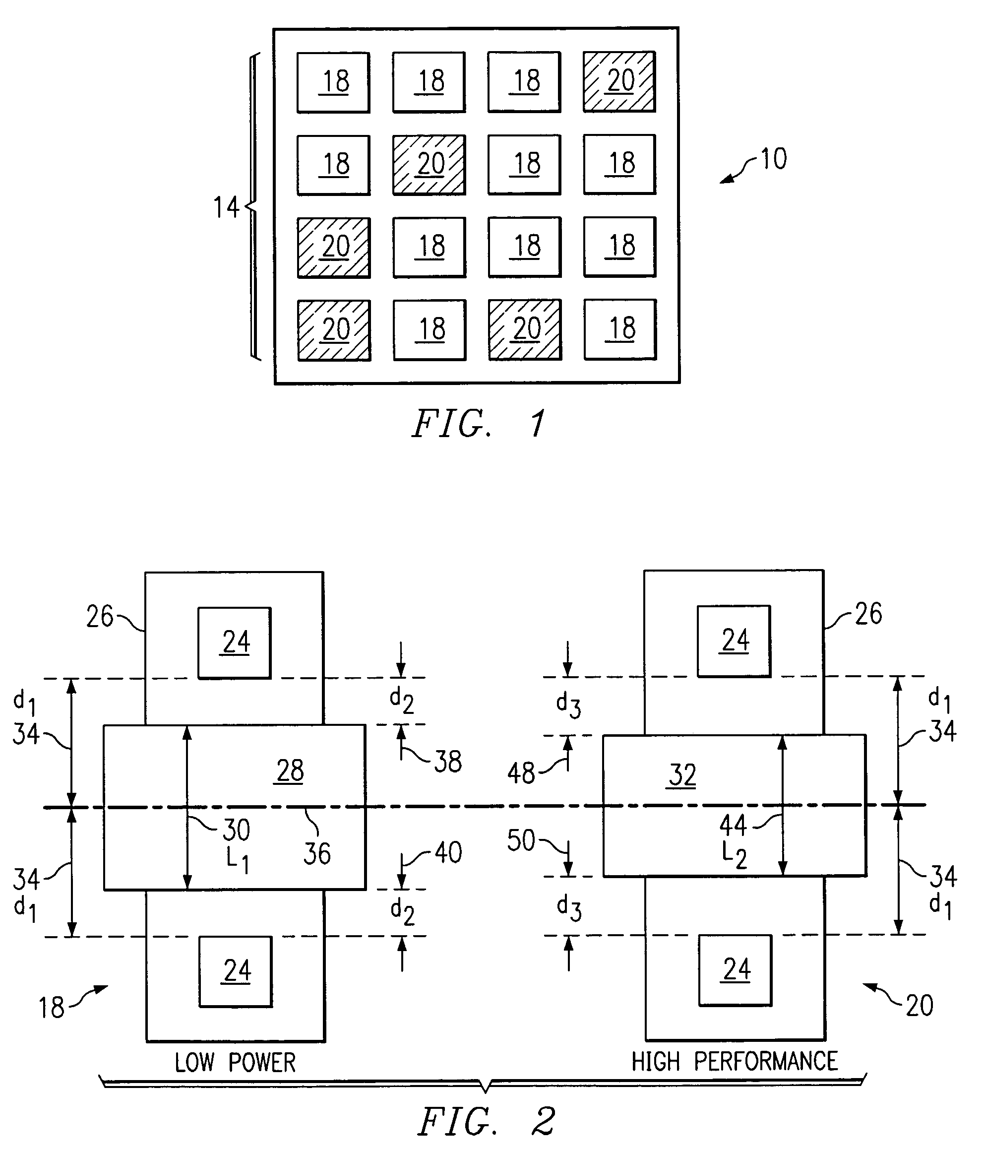
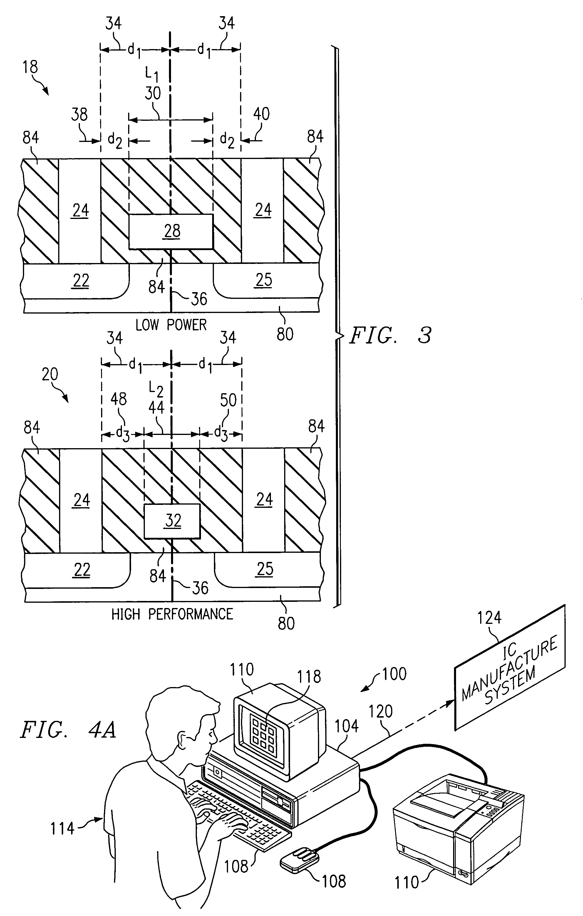
[0016]FIG. 1 illustrates a block diagram of an embodiment of an integrated circuit 10 having a plurality of cells 14. A “cell” refers to a specific layout of a set of elements, such as an interconnection of transistors to perform a logic function. A cell may include one or more transistors. Examples of cells 14 include a 3-input NAND or a flip-flop. Each cell 14 may have different levels of performance and leakage current. For example, as illustrated in FIG. 1, cells 14 may include low power cells 18 and high performance cells 20. A “low power cell,” such as low power cell 18, is a cell that has one or more features for reducing quiescent leakage current (“IDDQ”) in exchange for degraded performance of the cell. An example of such a feature is a gate having a relatively longer length, which narrows...


PUM


Abstract

According to one embodiment of the invention, a method for designing an integrated circuit is provided. The method includes providing a first transistor in a first logic path. The first transistor has a first contact, a first gate length and a first contact to gate centerline spacing. The method also includes providing a second transistor in a second logic path. The second transistor has a second contact, a second gate length and a second contact to gate centerline spacing. The first contact to gate centerline spacing is substantially equal to the second contact to gate centerline spacing. The method also includes selecting a different gate length for the first gate length using a predetermined design criterion.

Description

TECHNICAL FIELD OF THE INVENTION[0001]This is a division of Application Ser. No. 10 / 233,352, filed Aug. 30, 2002 and now U.S. Pat. No. 6,734,521, the entire disclosure of which is hereby incorporated by reference.CROSS-REFERENCE TO RELATED APPLICATIONS[0002]This application is related to U.S. Pat. No. 6,687,145 (Ser. No. 10 / 028,199, filed Dec. 20, 2001) entitled “Static Random Access Memory Cell and Methods”. With its mention in this section, this patent application is not admitted to be prior art with respect to the present invention.BACKGROUND OF THE INVENTION[0003]Reduction of quiescent leakage current (“IDDQ”) in integrated circuits (“IC”), such as an application specific integrated circuit (“ASIC”), is one goal of integrated circuit design because such a reduction lowers the overall power consumption of the IC. However, implementing features in cells of the IC to reduce the IDDQ also degrades the performance of the cells. Because of the performance degradation, these cells, ref...

Claims


Application Information

Patent Timeline
IPC IPC(8): H01L21/70H01L21/8234H01L27/118
CPCH01L21/823456H01L27/11803
Inventor HOUSTON, THEODORE W.
Owner TEXAS INSTR INC
Learn More