DDR memory modules with input buffers driving split traces with trace-impedance matching at trace junctions

a memory module and split tracing technology, applied in the field of buffering signals on memory modules, can solve the problems of large capacitance load on the inputs of memory modules,

Inactive Publication Date: 2005-09-20
DIODES INC
View PDF14 Cites 18 Cited by
  • Summary
  • Abstract
  • Description
  • Claims
  • Application Information

AI Technical Summary

Problems solved by technology

These DRAM-input capacitances can be significant, producing a large capacitive load on the inputs to the memory modules, especially when many DRAM chips are mounted on the same memory module.
Further compounding the input-capacitance problem is the use of expansion memory.
FIG. 2 highlights a reflection problem caused by trace junctions.
These reflections disturb instantaneous voltages along the line, and take time to settle.
This settling time can reduce the practical operating frequency.
Termination circuits such as resistors are normally added to trace endpoints on other systems, but memory modules are so small that such terminations are not practical.

Method used


Image

  • DDR memory modules with input buffers driving split traces with trace-impedance matching at trace junctions
  • DDR memory modules with input buffers driving split traces with trace-impedance matching at trace junctions
  • DDR memory modules with input buffers driving split traces with trace-impedance matching at trace junctions

Examples


Embodiment Construction

[0027]The present invention relates to an improvement in memory modules. The following description is presented to enable one of ordinary skill in the art to make and use the invention as provided in the context of a particular application and its requirements. Various modifications to the preferred embodiment will be apparent to those with skill in the art, and the general principles defined herein may be applied to other embodiments. Therefore, the present invention is not intended to be limited to the particular embodiments shown and described, but is to be accorded the widest scope consistent with the principles and novel features herein disclosed.

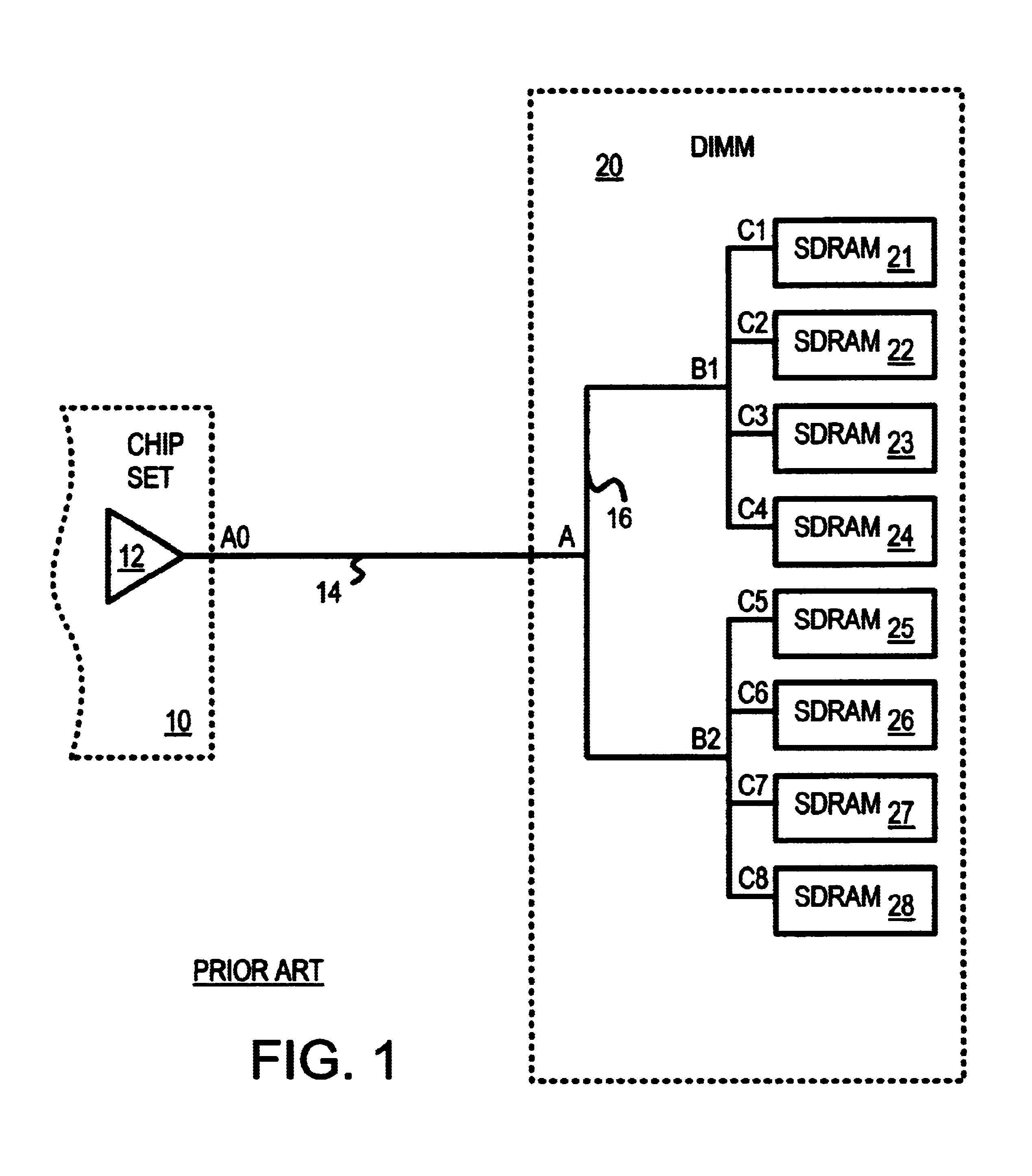
[0028]FIG. 4 highlights the concept of impedance matching at a wiring-trace junction on a memory module. An incoming signal, such as address A0 from a memory controller chip set, passes through the memory module socket and enters the memory module on input line 15. At junction A, input line 15 splits into two branches (lines 16) to sec...


PUM


Abstract

A memory module has improved signal propagation delays for signals externally driven such as from a motherboard. Reflections from junctions of wiring traces on the memory module are reduced or eliminated. An input buffer or register receives a signal from the motherboard and splits the signal to drive two outputs to two separate traces. Each trace is enlarged in width or thickness, such as by using a double-width wiring trace. At the fare end of each double-width trace, a junction is made to two minimum-width traces that connect to small stub traces to DRAM inputs. Reflections from the junction are eliminated or reduced by trace-impedance matching, since the input impedance of the double-width trace from the input buffer is about the same as the combined impedance of the two minimum-width traces. Trace-input matching and input buffering can improve signal integrity and overall propagation delay.

Description

BACKGROUND OF INVENTION[0001]This invention relates to memory modules, and more particularly to buffering signals on memory modules.[0002]Memory modules such as dual-inline memory modules (DIMMs) are widely used in electronic systems such as personal computers (PCs). Memory modules have memory chips such as dynamic-random-access memories (DRAMs) mounted on a small substrate such as a printed-circuit board (PCB). Contact pads are formed along one edge of the substrate to make electrical contact when the memory module is plugged into a socket such as on a PC motherboard.[0003]As these electronic systems operate at higher and higher speeds, signals driven to the memory modules must also operate at higher frequencies. Faster high-current drivers can be used to more rapidly drive current to charge and discharge the capacitances on the inputs of DRAM chips on the memory modules. These DRAM-input capacitances can be significant, producing a large capacitive load on the inputs to the memory...

Claims


Application Information

Patent Timeline
Patent Type & Authority Patents(United States)
IPC IPC(8): G11C5/06G11C7/10H05K1/02
CPCG11C5/04G11C5/063G11C7/1072H05K1/025H05K1/0245H05K2201/09254H05K2201/09727
Inventor YEN, YAO TUNG
Owner DIODES INC
Why Eureka
Try Eureka