
Flash memory cell with drain and source formed by diffusion of a dopant from a silicide

a technology of flash memory cells and diffusion channels, applied in the field of flash memory cell drain and source fabrication systems, can solve the problems of difficult to achieve optimized results within requisite narrow tolerances, complicated process for flash memory devices, and difficult to achieve etc., to facilitate the reduction of drain induced barrier (dibl), facilitate efficient fabrication of flash memory cells, and reduce the probability of region alignment or shift problems

Inactive Publication Date: 2005-09-13
MONTEREY RES LLC
View PDF2 Cites 6 Cited by
  • Summary
  • Abstract
  • Description
  • Claims
  • Application Information

AI Technical Summary

Benefits of technology

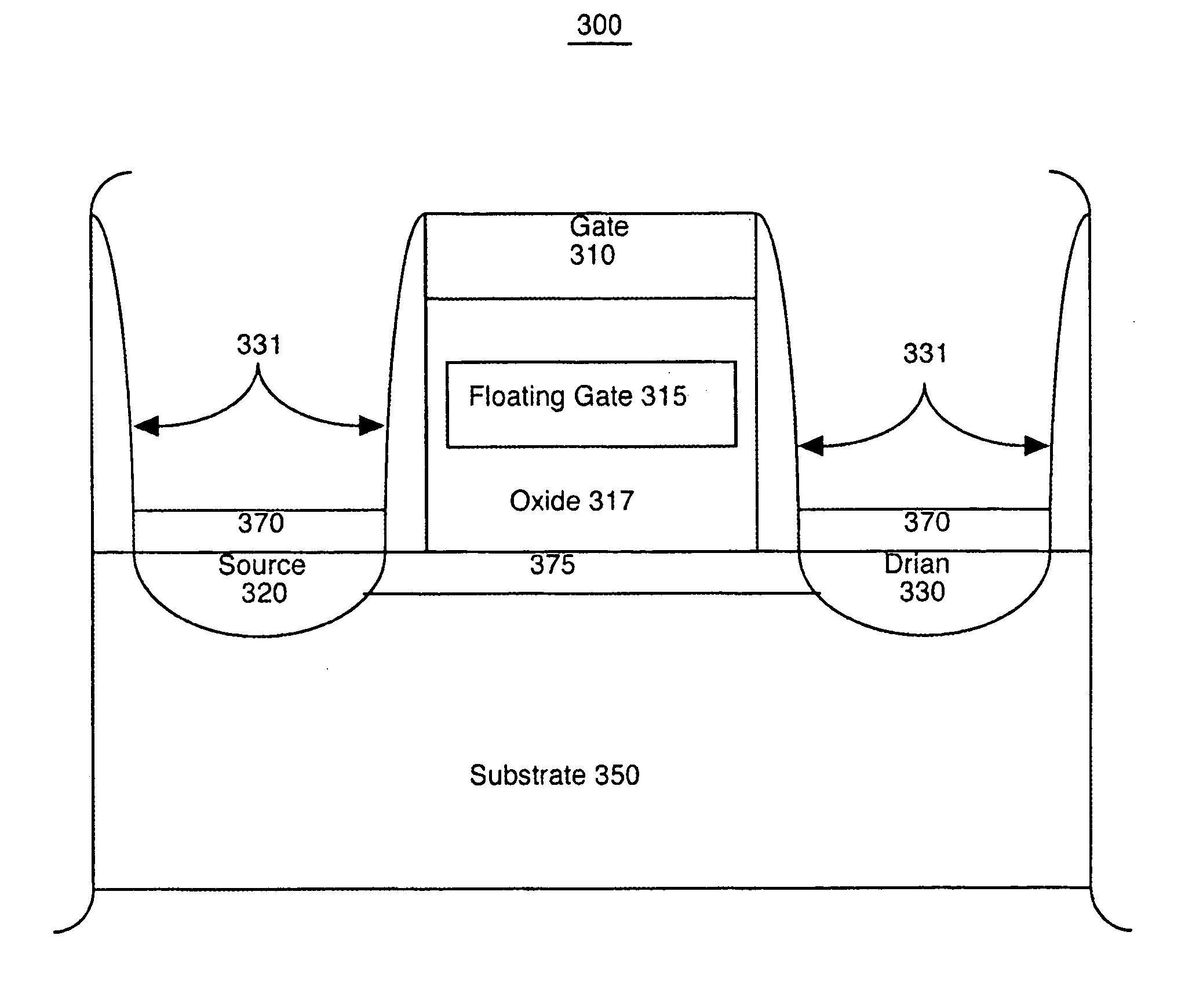
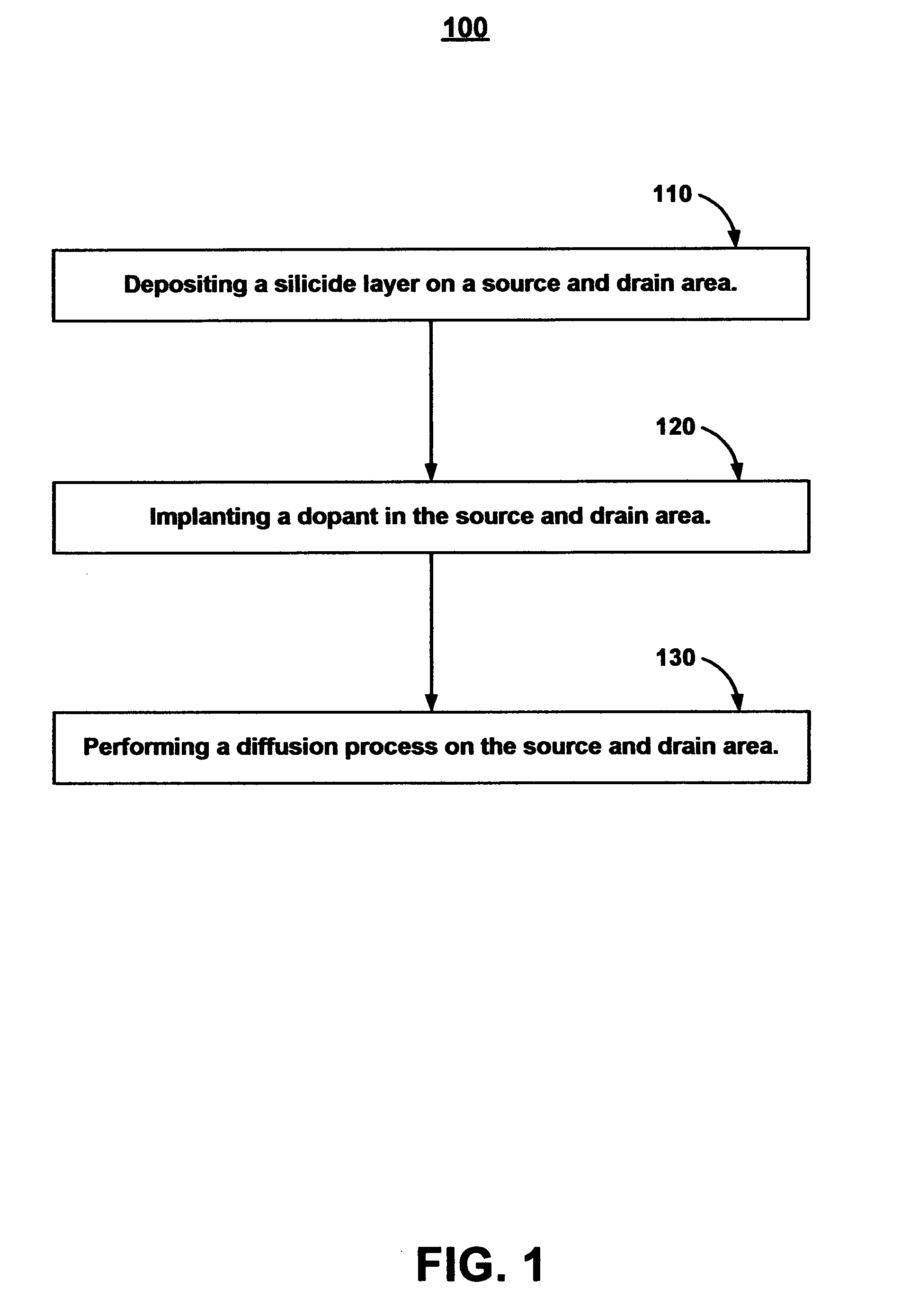
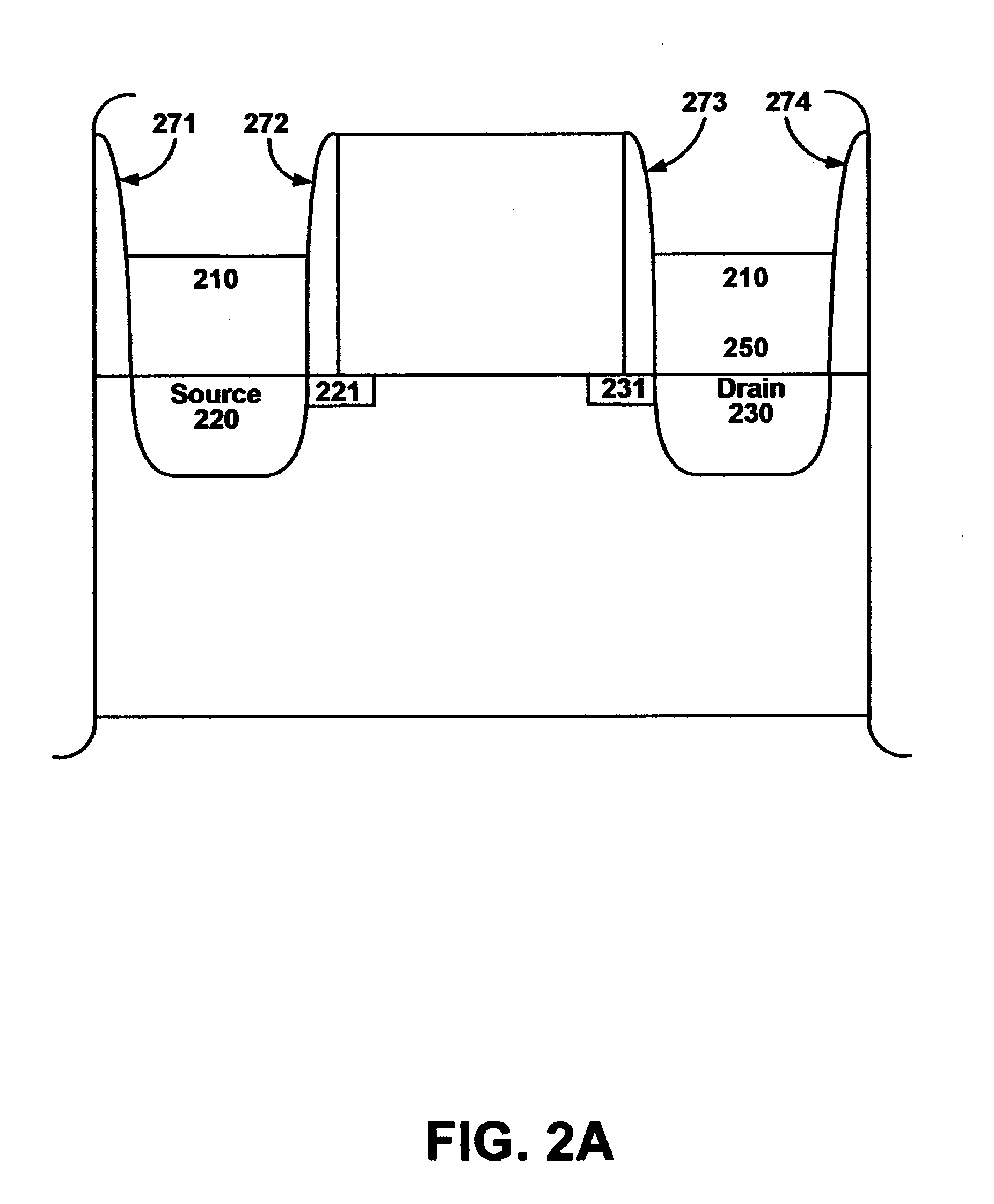
[0009]The present invention is a flash memory manufacturing process that facilitates efficient fabrication of a flash memory cell. In one embodiment, a silicide (e.g., CoSi) is utilized as a diffusion source. A layer of silicide is deposited over a source area and drain area. The silicide, source area and drain area are implanted with a dopant (e.g., arsenic). The wafer is then subjected to a diffusion process which forces the dopants from the silicide into the source area and drain area. The diffusion process can be performed at relatively low temperatures reducing the probability of region alignment or shift problems. The present invention also enables shallow source and drain junction formation in a manner that facilitates reduced drain induced barrier lowering (DIBL) and reduced source to drain resistance. In addition, utilizing the silicide as a diffusion source enables the use of narrower side wall spacers (e.g., nitride spacers) permitting a greater number of components concentrated in smaller areas.

Problems solved by technology

The fabrication of memory devices often involves complex processes that require precise operations to achieve desired delicate balances.
The ability to access a memory and transfer information quickly and conveniently usually has a significant impact on information processing latency and often limits the utility a device can provide.
Many integrated circuit processes involve repeated deposition and removal of material layers to fabricate components and it is often very difficult to achieve optimized results within requisite narrow tolerances.
These regions can be adversely impacted by subsequent process steps in a manner that significantly affects performance.
In typical traditional processes, dopants are implanted directly into the silicon (Si), which causes damage in the Si.
For example, high temperature annealing can result in diffusion region migration that adversely changes the characteristics of a source or drain junction (e.g., resistivity, drain induced barrier leakage, etc.).
Semiconductor integrated circuit manufacturing efforts are usually complicated by ever increasing demands for greater functionality.
More complicated circuits are usually required to satisfy the demand for greater functionality.
However, including more components within an integrated circuit often requires the components to be densely packed in relatively small areas and reliably packing a lot of components in relatively small areas of an IC is usually very difficult.
Diffusion of high quality dopants with the ability to provide shallow junctions can be challenging.
The implantation energy usually has to be high to ensure the CoSi layer is above N+ / P junction, which often results in a deeper junction and worse DIBL.

Method used


Image

  • Flash memory cell with drain and source formed by diffusion of a dopant from a silicide
  • Flash memory cell with drain and source formed by diffusion of a dopant from a silicide
  • Flash memory cell with drain and source formed by diffusion of a dopant from a silicide

Examples


Embodiment Construction

[0016]Reference will now be made in detail to the preferred embodiments of the invention, examples of which are illustrated in the accompanying drawings. While the invention will be described in conjunction with the preferred embodiments, it will be understood that they are not intended to limit the invention to these embodiments. On the contrary, the invention is intended to cover alternatives, modifications and equivalents, which may be included within the spirit and scope of the invention as defined by the appended claims. Furthermore, in the following detailed description of the present invention, numerous specific details are set forth in order to provide a thorough understanding of the present invention. However, it will be obvious to one ordinarily skilled in the art that the present invention may be practiced without these specific details. In other instances, well known methods, procedures, components, and circuits have not been described in detail as not to unnecessarily o...


PUM


Abstract

The present invention is a flash memory manufacturing process that facilitates efficient fabrication of a flash memory cell. In one embodiment, a silicide (e.g., CoSi) is utilized as a diffusion source. A layer of silicide is deposited over a source area and drain area. The dopant is implanted into the CoSi and diffuse out conformably along CoSi-Si interface at a relatively low temperature. The low temperature diffusion facilitates fabrication of a Flash core cell with a very shallow source / drain junction, and as a result a robust DIBL. The present invention also facilitates fabrication of memory cells with smaller spacers and shorter gate length.

Description

TECHNICAL FIELD[0001]The present claimed invention relates to the field of memory fabrication. More particularly, the present invention relates to a flash memory cell drain and source fabrication system and method that utilizes silicide as a diffusion source.BACKGROUND ART[0002]Electronic systems and circuits have made a significant contribution towards the advancement of modern society and are utilized in a number of applications to achieve advantageous results. Numerous electronic technologies such as digital computers, calculators, audio devices, video equipment, and telephone systems have facilitated increased productivity and reduced costs in analyzing and communicating data, ideas and trends in most areas of business, science, education and entertainment. Frequently, these advantageous results are realized through the use of information stored on a memory media and manipulated by a processing device. The fabrication of memory devices often involves complex processes that requi...

Claims


Application Information

Patent Timeline
Patent Type & Authority Patents(United States)
IPC IPC(8): H01L29/66H01L29/788
CPCH01L21/28273H01L29/0847H01L29/0891H01L29/42324H01L29/66825H01L29/7881H01L29/40114
Inventor FANG, SHENQING
Owner MONTEREY RES LLC
Learn More