BiCMOS technology on SOI substrates

a technology of bipolar and complementary metal oxide semiconductors, applied in the direction of semiconductor devices, electrical apparatus, transistors, etc., can solve the problems of device performance degradation, serious device operational limitations, and low efficiency, and achieve the effect of simple yet reliabl

Inactive Publication Date: 2005-08-30
GLOBALFOUNDRIES US INC
View PDF25 Cites 45 Cited by
  • Summary
  • Abstract
  • Description
  • Claims
  • Application Information

AI Technical Summary

Benefits of technology

[0020]One object of the present invention is to provide a simple, yet reliable method of fabricating a high-performance HBT in an integrated BiCMOS process in which the topography between the HBT device area and the CMOS device area is substantially the same.
[0023]These and other objects and advantages are achieved in the present invention by utilizing a method in which the HBT is built in an area in which the top Si-containing and the buried insulating layer of an SOI substrate have been selectively etched. That is, in the present invention, the HBT is built directly atop an upper surface of a bottom Si-containing layer of an SOI substrate. The inventive method thus decouples the substrate for the CMOS transistors and the HBTs. An optional proton ion implant step can be performed in areas of the SOI substrate that are periphery to either the HBT device area or the CMOS device area to increase the substrate resistance for subsequent formation of a high-Q inductor.
[0028]In some embodiments of the present invention, portions of the SOI substrate that lay in the periphery of the extrinsic base heterojunction bipolar transistor are subjected to a proton ion implant step, which increases the resistance of the SOI substrate to provide areas for fabricating inductors having a high-Q factor.
[0029]In another embodiment of the present invention, the portion of the upper silicon-containing layer is removed from the region of the SOI substrate in which the bipolar device is subsequently formed and is replaced with an insulating material. The insulating material defines the bipolar region of the substrate. This method of the present invention, can reduce the number of masking steps utilized to provide a heterojunction bipolar device. In broad terms, this method of the present invention includes:

Problems solved by technology

As the vertical dimensions of the bipolar transistor are scaled more and more, serious device operational limitations have been encountered.
The ion implantation will cause damage, however, to the base region.
Such damage may ultimately lead to degradation in device performance.
The selective epitaxy with a cavity structure mandates stringent process requirements for good selectivity, and suffers from poor process control.
However, when it comes to SiGe BiCMOS structures, there is a topographic issue for CMP since the CMOS gate creates a thickness difference, which is similar to the gate height (typically 100-250 nm), between the CMOS device area and the bipolar transistor device area.
Despite being capable of leveling the two device areas, this prior art approach for adjusting the height differential between the HBT and the CMOS transistor device areas is complicated and requires two additional lithographic levels to achieve leveling between the device areas of the CMOS transistor and the HBT.
Despite being capable of fabricating a bipolar transistor on an SOI substrate, this prior art approach needs a selective epitaxial silicon growth process which mandates stringent process requirements for good selectivity, and suffers from poor process control.
Moreover, the form factor of the entire prior art bipolar transistors inherently lacks the compactness of the state-of-the art bipolar transistors in advanced BiCMOS technologies, e.g., the entire base region is separated from the collector by oxide sidewalls.
This makes it difficult to reduce the product of base-collector capacitance and collector resistance, which is critical to enable fast bipolar transistors.
Not only does this etch create damage in Si, rendering defective epitaxial base layer later on, but also it is not controllable; therefore the depth of the trenches for bipolar transistors formed into the SOI substrate may vary from one area to another as well as vary across a single SOI wafer.
This results in a topography problem with each bipolar transistor being formed using technology such as disclosed in Lee.
Another challenge facing BiCMOS device fabrication is that different devices present on the same chip have different substrate requirements.

Method used


Image

  • BiCMOS technology on SOI substrates
  • BiCMOS technology on SOI substrates
  • BiCMOS technology on SOI substrates

Examples


Embodiment Construction

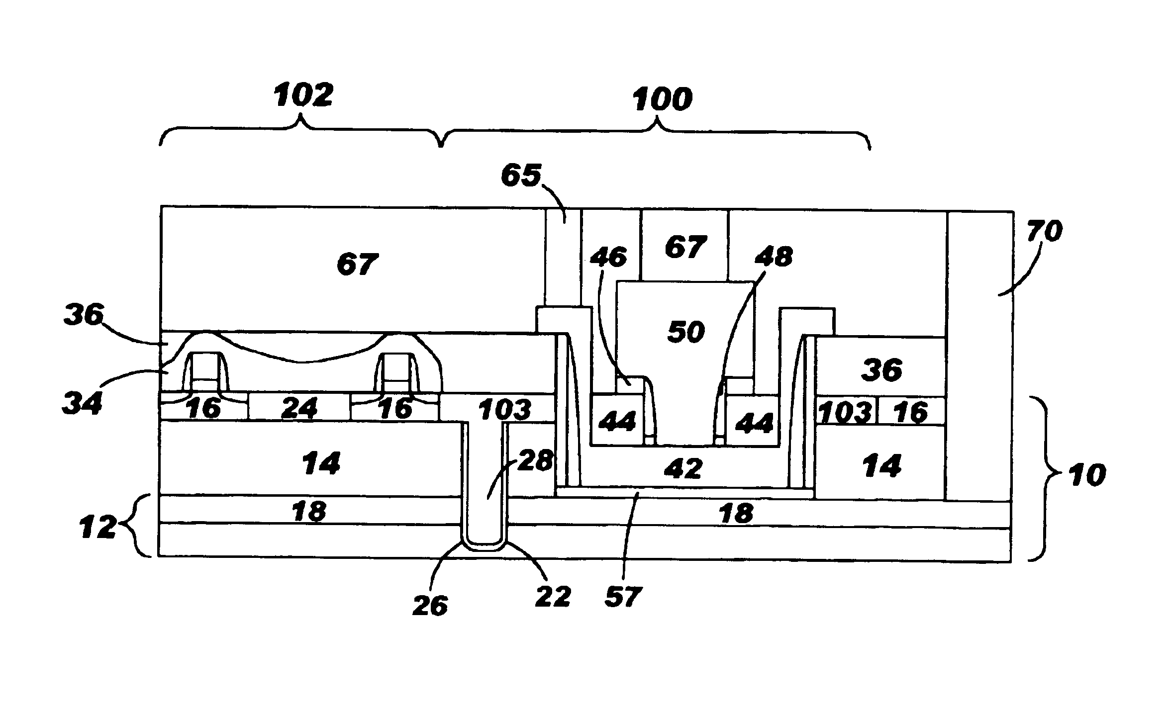
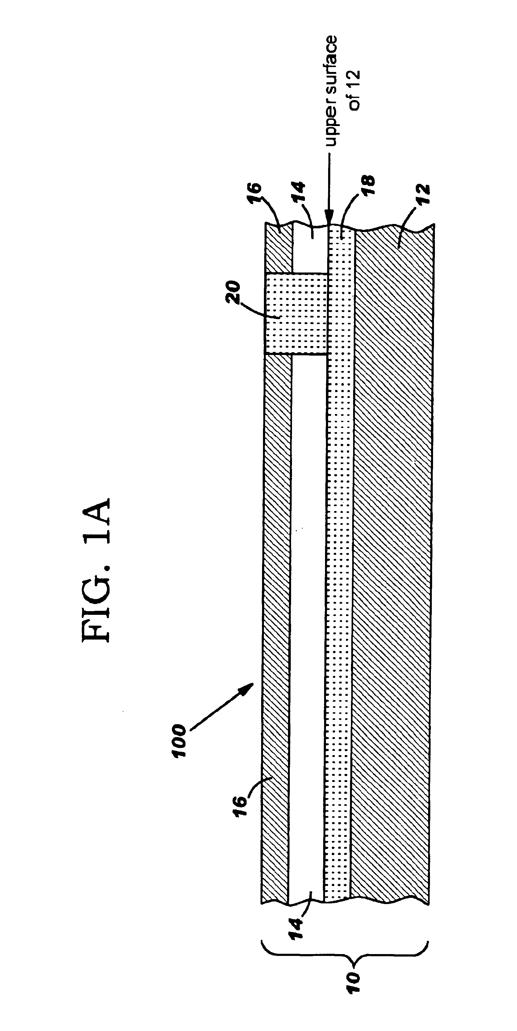
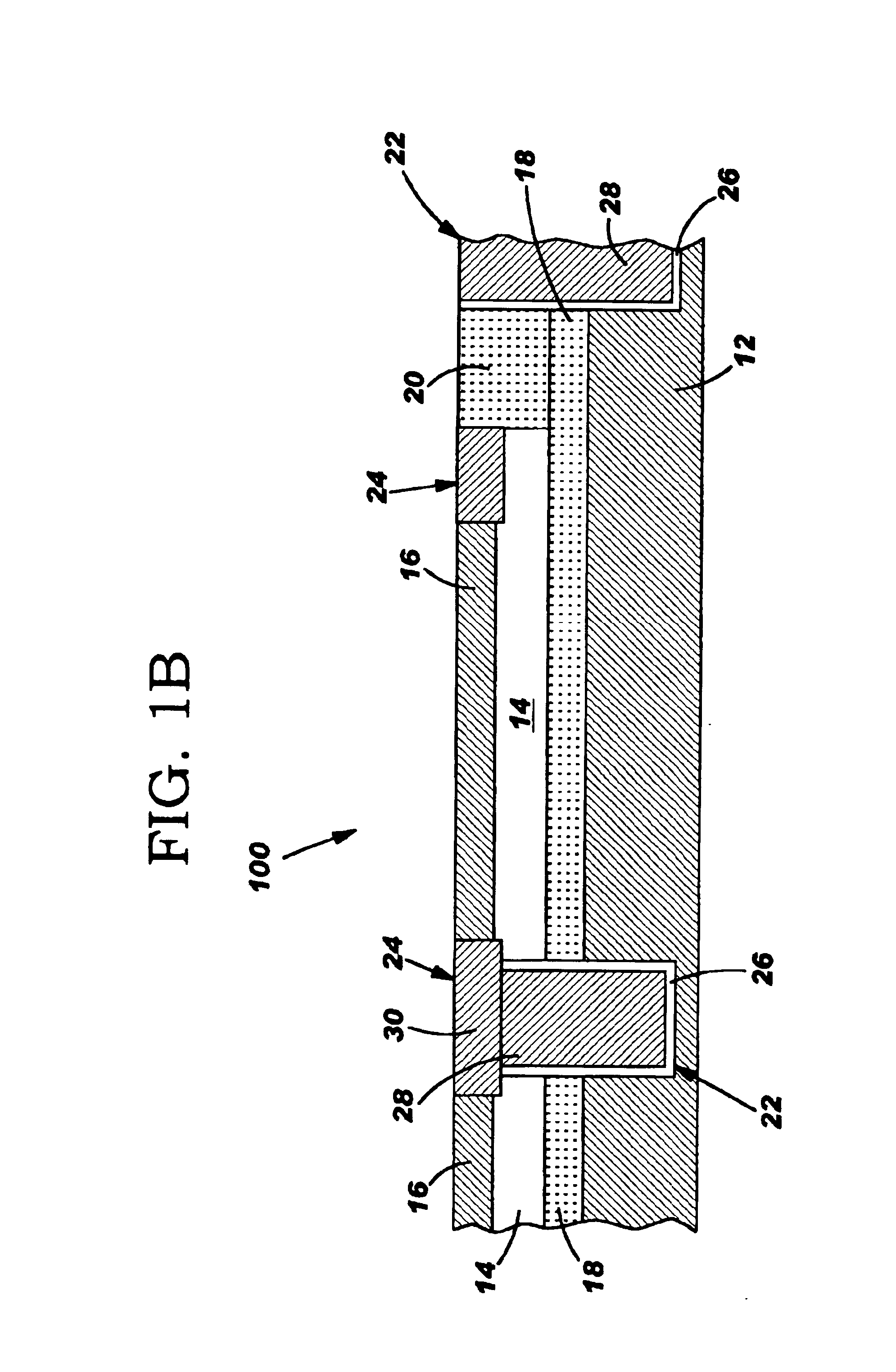
[0043]The present invention, which provides a method of integrating, BiCMOS technology with SOI technology, will now be described in greater detail by referring to the drawings that accompany the present application. The drawings shown in FIGS. 1A-1G only depict the HBT device area 100. For clarity, the CMOS device areas as well as the other areas of a typical BiCMOS structure are not shown in FIGS. 1A-1G. In FIG. 2 of the present application, an HBT device area 100, a CMOS device area 102 and a passive device area 104 are shown. FIGS. 3A-3M depict the HBT device area 100 and the CMOS device area 102.

[0044]Reference is first made to the initial structure shown in FIG. 1A; the bipolar device region 100 is shown; the CMOS device region 102 and the passive device region 104 are not shown for clarity. Despite not being shown, the CMOS device region and the passive device region would lay to the periphery of the bipolar device region 100 shown in FIGS. 1A-1G. Although a single bipolar de...


PUM


Abstract

A method and a BICMOS structure are provided. The BiCMOS structure includes an SOI substrate having a bottom Si-containing layer, a buried insulating layer located atop the bottom Si-containing layer, a top Si-containing layer atop the buried insulating layer and a sub-collector which is located in an upper surface of the bottom Si-containing layer. The sub-collector is in contact with a bottom surface of the buried insulating layer. The structure also includes an extrinsic base heterojunction bipolar transistor located in an opening provided in a bipolar device area of the SOI substrate in which a base region of the bipolar transistor is located directly atop the sub-collector

Description

CROSS REFERENCE TO RELATED APPLICATIONS[0001]This application is a continuation-in-part of U.S. patent application Ser. No. 10 / 249,819 entitled BiCMOS TECHNOLOGY ON SOI SUBSTRATES, filed May 9, 2003, the entire content and subject matter of which are incorporated herein by reference.BACKGROUND OF INVENTION[0002]1. Field of the Invention[0003]The present invention relates to integrated bipolar and complementary metal oxide semiconductor (BiCMOS) devices using silicon-on-insulator (SOI) technology in which the bipolar transistors and the CMOS transistors are fabricated on different surface layers of the SOI substrate. The present invention also provides a method for forming the BiCMOS devices. The structure and method of the present invention overcome topographic challenges as well as providing different surface layers in the SOI substrate for fabricating the various devices present in BiCMOS technology.[0004]2. Background of the Invention[0005]Bipolar transistors are electronic devic...

Claims


Application Information

Patent Timeline
IPC IPC(8): H01L21/331H01L21/02H01L29/00H01L31/0264H01L31/0328H01L27/01H01L27/06H01L27/12
CPCH01L27/1203H01L29/66242H01L29/66265H01L27/0623H01L29/7371H01L29/0653H01L21/76264
Inventor ELLIS-MONAGHAN, JOHN JOSEPHJOSEPH, ALVIN JOSELIU, QIZHIPETERSON, KIRK DAVID
Owner GLOBALFOUNDRIES US INC
Why Eureka
Try Eureka