
Electronic package and method of forming

a technology of electronic packaging and semiconductor chips, applied in the direction of semiconductor devices, semiconductor/solid-state device details, electrical apparatus, etc., can solve the problems of increasing the thermal resistance of the interface, affecting the operation of the device, and the maximum allowed thermal degradation, so as to improve the operational field life, improve the operating field life, and reduce the interfacial stress

Inactive Publication Date: 2005-08-23
GLOBALFOUNDRIES INC
View PDF17 Cites 34 Cited by
  • Summary
  • Abstract
  • Description
  • Claims
  • Application Information

AI Technical Summary

Benefits of technology

[0009]It is yet another object of this invention to provide an electronic package that minimizes interfacial stresses between the adhesive and both the chip and a cover or cap over the chip and results in much improved operational field life.
[0010]Still another object of this invention is to provide an electronic package that does not require the presence or use of thermal grease and has superior thermal performance.

Problems solved by technology

However, any cover, cap, or encapsulant above the chip increases the thermal resistance path to an ambient environment and, hence, the operational temperature of the chip.
However, it has been found that during thermal cycling, the grease has a tendency to be pumped, or displaced from the interface between the chip and the cap, thus increasing the thermal resistance of the interface.
Pumping, or grease pumping as it is commonly referred, results as the gap between the chip and the cap increases and decreases, eventually forcing enough grease out of the gap, and forming a critical number of voids, to hinder thermal performance.
A critical magnitude of tensile / compressive grease strain exists which results in maximum allowed thermal degradation.
This approach is not, however, without problems.
The CTE mismatch between the chip and the cap produces interfacial stresses between the adhesive and both the surface of the cap and the top surface of the chip.
These stresses can cause delamination during the manufacturing process or during thermal cycling (chip operation in the field) near the corners and edges of the chip.
Once delamination begins, crack propagation may ultimately lead to a defective product and / or electrical failure in the field.
This is a major problem with capped chips particularly with flip chips on circuitized substrates of the organic type, such as epoxy laminate types.

Method used


Image

  • Electronic package and method of forming
  • Electronic package and method of forming
  • Electronic package and method of forming

Examples


Embodiment Construction

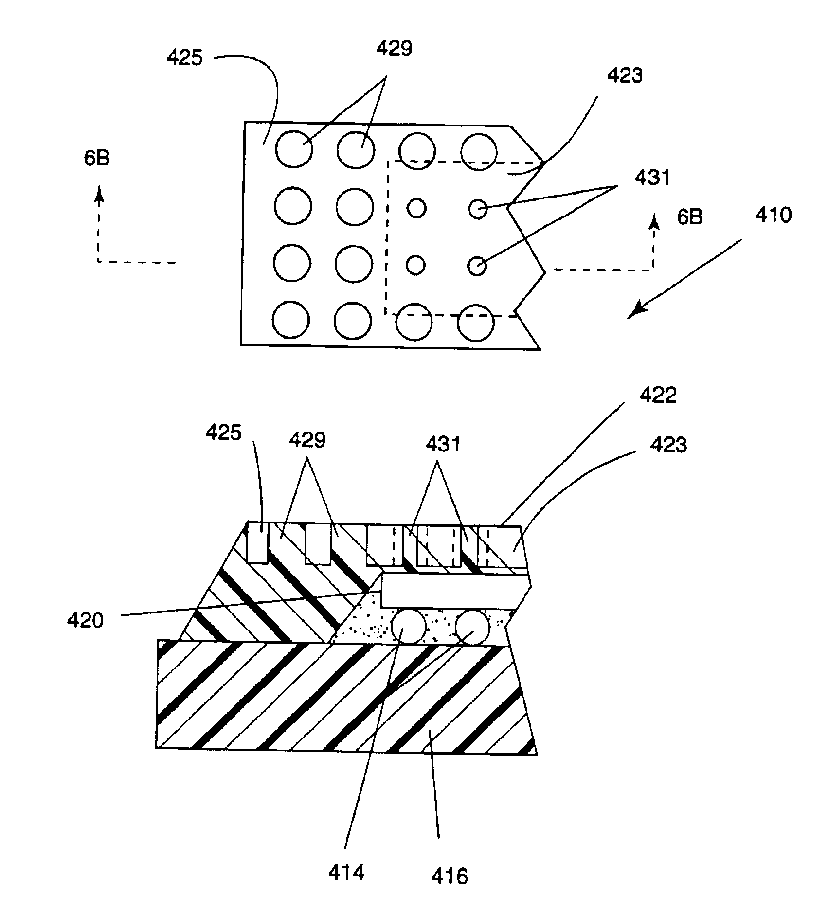
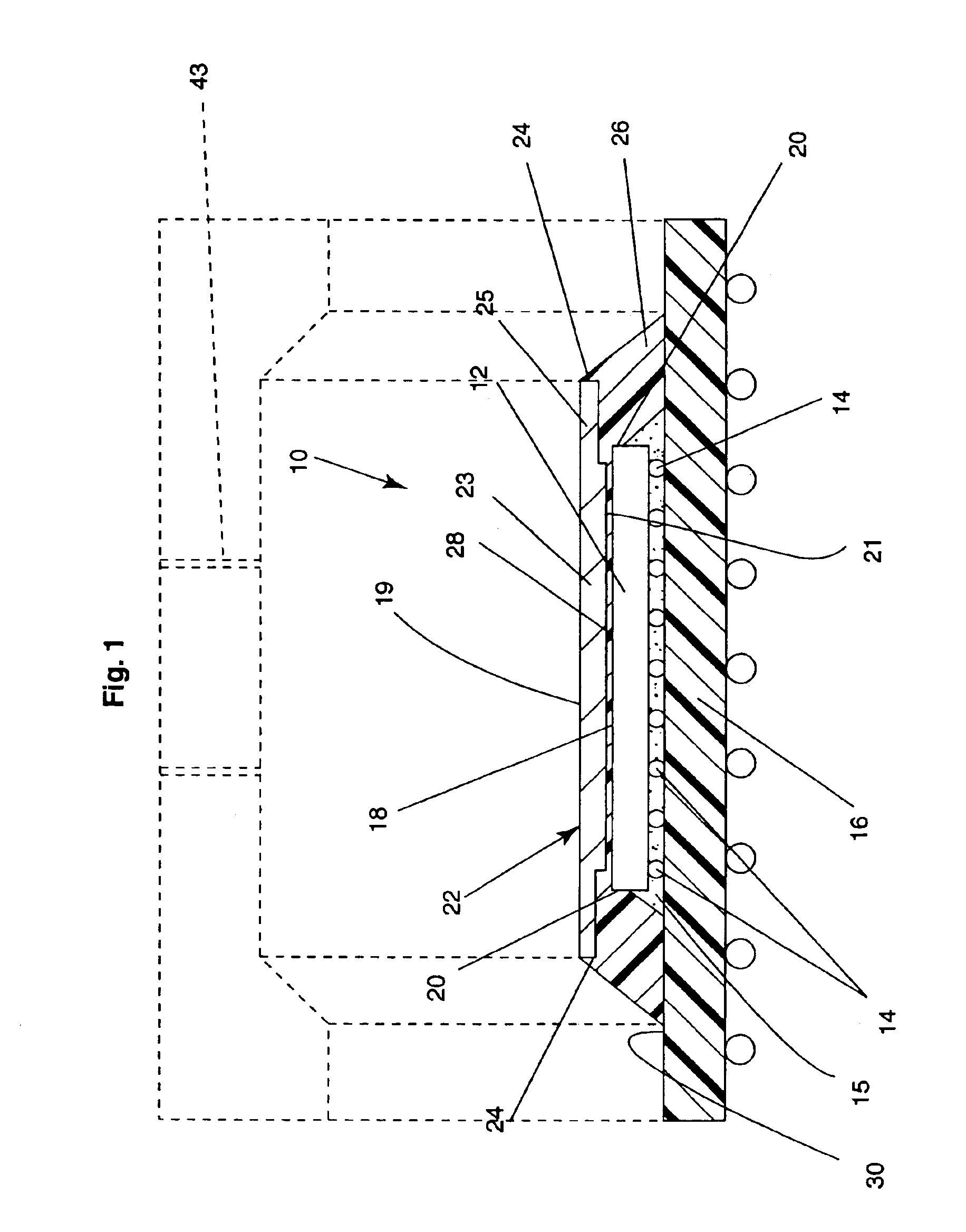
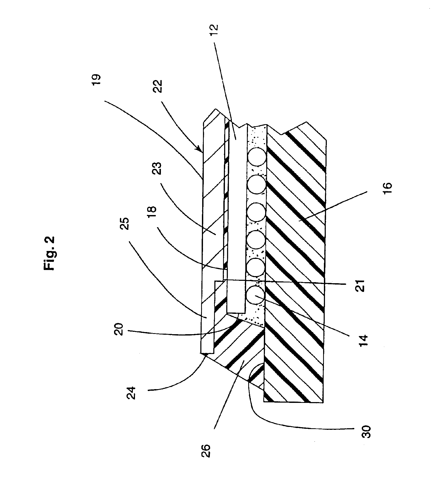
[0029]An electronic package 10 embodying the present invention, is shown in FIG. 1. The electronic package includes a chip 12, (e.g., a flip chip), that has a plurality of electrical contacts 14 (e.g., solder balls) that are electrically connected to corresponding contacts associated with one or more electrical circuits disposed on a circuitized substrate 16. If desired, an underfill material 15 such as Dexter Hysol™ 4511 epoxy, made by Dexter Electronic Materials, Industry, CA, may be used to prolong fatigue life of electrical contacts 14. Other commercially available underfill materials that can be used are available from Dexter Electronic Materials as Dexter Hysol™ 4527 or from Namics Corporation, Niigata City, Japan, under the product name Namics 8437-2. The circuitized substrate 16 is a circuit board having a number of electrical circuits defined on and within the substrate and is adapted for interconnection with other components of an electronic assembly. The circuit board can...


PUM


Abstract

An electronic package and method of making same in which a thermally conductive member is in thermally conductive communication with a semiconductor chip encapsulated within a dielectric material that surrounds portions of a thermally conductive member, semiconductor chip, and a predefined portion of a circuitized substrate. The present invention's thermally conductive member includes two portions of different bending stiffness to assure reduced interfacial stresses between the semiconductor chip and the circuitized substrate.

Description

CROSS REFERENCE TO APPLICATIONS[0001]This application is a divisional application of Ser. No. 09 / 430,075, filed Oct. 29, 1999, now U.S. Pat. No. 6,507,116 which is a continuation in part of Ser. No. 09 / 080,117, filed May 15, 1998, now U.S. Pat. No. 6,104,093, which is a continuation in part of Ser. No. 08 / 842,417, filed Apr. 24, 1997, now U.S. Pat. No. 5,883,430.TECHNICAL FIELD[0002]This invention relates generally to encapsulated semiconductor chips and more particularly to a semiconductor chip package, an electronic package, such as a flip chip package, having a thermally conductive member encapsulated with the semiconductor chip.BACKGROUND OF THE INVENTION[0003]A flip chip is a small semiconductor chip (chip) having terminations all on one side in the form of solder pads or bump contacts. Typically, the surface of the chip has been passivated or otherwise treated. The flip chip derives its name from the practice of flipping, or turning, the chip over after manufacture, prior to a...

Claims


Application Information

Patent Timeline
Patent Type & Authority Patents(United States)
IPC IPC(8): H01L23/34H01L23/31H01L23/28H01L23/433
CPCH01L23/3128H01L23/4334H01L2224/73204H01L2924/01004H01L2924/0102H01L2924/15311H01L2224/16225H01L2224/32225H01L2924/00H01L2224/73253H01L2224/32245
Inventor CALETKA, DAVID V.JOHNSON, ERIC A.
Owner GLOBALFOUNDRIES INC
Learn More