Film bulk acoustic resonator

Inactive Publication Date: 2005-08-16
TAIYO YUDEN KK
View PDF14 Cites 10 Cited by
  • Summary
  • Abstract
  • Description
  • Claims
  • Application Information

AI Technical Summary

Benefits of technology

[0012]The present invention has been proposed under the circumstances described above. It is, therefore, an object of the present invention is to provide an FBAR fabrication method and an FBAR itself that are capable of overcoming or at least alleviating the conventional problems. In particular, the present invention aims to provide an FBAR wherein an underlying hollow portion can be formed without relying on the time-consuming grinding of the sacrificial layer.

Problems solved by technology

A problem of a SAW filter is that the comb-teeth electrode may be distorted, and even broken, due to the elastic waves resulting from the application of high voltage.
This drawback becomes conspicuous as the comb-teeth electrode is smaller in width, that is, as the filter is designed to deal with higher frequencies.
The above conventional techniques suffer from the following problems.
Such fragility may require for extra care in dealing with the silicon wafer (e.g. in transporting the wafer from one working spot to another spot), and may lower the production yield rate.
Another problem is caused by the etching process which renders the hollow portion to flare out in the downward direction.
With such a hollow portion varying in diameter in the thickness direction of the wafer, the respective resonators constructing a ladder-form filter tend to be unduly bulky.
Thus, according to the teaching of JP-A-2000-69594, a resulting resonator is rather expensive due to the increased production costs.
However, this document does not specifically show a method of making the hollow portion nor a method of making an FBAR.

Method used


Image

  • Film bulk acoustic resonator
  • Film bulk acoustic resonator
  • Film bulk acoustic resonator

Examples


first embodiment

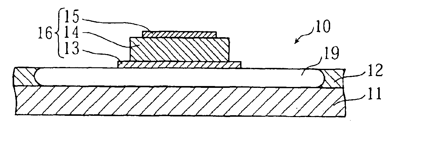
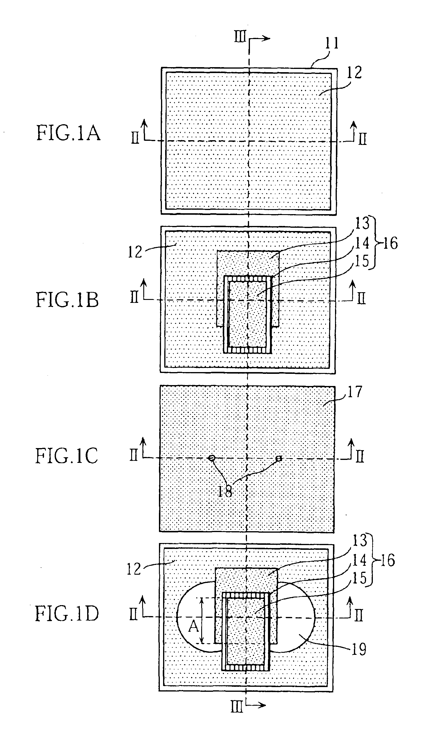
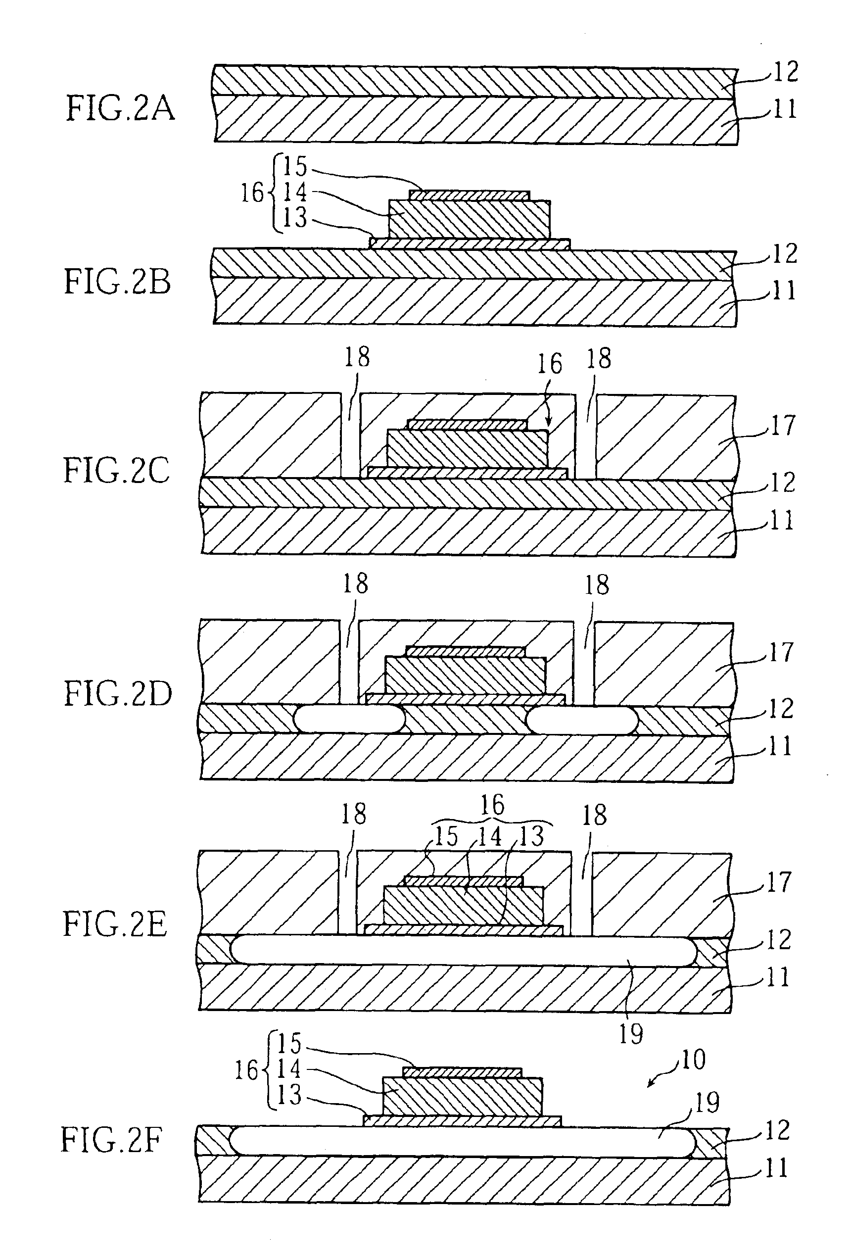
[0039]Reference is first made to FIGS. 1A-1D, 2A-2F and 3A-3F to describe an FBAR (Film Bulk Acoustic Resonator) fabrication method according to the present invention. As noted above, FIGS. 1 are plan views, FIGS. 2 are sectional views taken along lines II—II in FIGS. 1, and FIGS. 3 are sectional views taken along lines III—III in FIGS. 1.

[0040]In accordance with the method, first, a base layer 12 is formed on a silicon substrate 11, as shown in FIGS. 1A, 2A and 3A. The base layer 12 has a thickness of 5 μm and is made of an insulating material such as magnesium oxide using a known sputtering for example. Of course, the present invention is not limited to this. For instance, the thickness of the base layer 12 may be varied in a range of 1-50 μm. The insulating material, other than magnesium oxide, may be silicon dioxide, zinc oxide, PSG (phosphorus-added silicon glass), BSG (boron-added silicon glass), BPSG (boron,phosphorus-added silicon glass), or SOG (spin-on glass).

[0041]Then, a...

second embodiment

[0048]Reference is now made to FIGS. 4A-4D, 5A-5F and 6A-6F to describe an FBAR fabrication method according to the present invention. Of these figures, FIGS. 4 are plan views, FIGS. 5 are sectional views taken along lines V—V in FIGS. 4, and FIGS. 6 are sectional views taken along lines VI—VI in FIGS. 4.

[0049]In accordance with the second embodiment, an FBAR is fabricated in the following manner. First, as shown in FIGS. 4A, 5A and 6A, a base layer 22 and a sacrificial layer 22′ are formed on a silicon substrate 21. Specifically, the base layer 22 may be made of silicon dioxide by plasma CVD (chemical vapor deposition) to have a thickness of 5 μm. Then, a magnesium oxide layer having a thickness of 10 nm is made on the base layer 22 by electron beam deposition for example. This MgO layer is processed into the sacrificial layer 22′ by photolithography and wet etching (or dry etching). For wet etching, the etchant may be acetic acid solution. In the illustrated embodiment, the sacrif...

fifth embodiment

[0061]FIGS. 9A-9F show the steps of an FBAR fabrication method according to the present invention. FIGS. 10A-10F are sectional views taken along lines X—X in FIGS. 9A-9F, while FIGS. 11A-11F are sectional views taken along lines XI—XI in FIGS. 9A-9F.

[0062]In accordance with the fifth embodiment, a base layer 52 and a sacrificial layer 52′ are formed on a silicon substrate 51, as shown in FIGS. 9A, 10A and 11A. Specifically, the base layer 52 is formed by providing a 5 μm-thick silicon oxide layer on the silicon substrate 51 by plasma CVD for example. Then, a 10 μm-thick magnesium oxide layer is formed on the base layer 52. Thereafter, the magnesium oxide layer is processed into the desired sacrificial layer 52′ by photolithography and wet (or dry) etching. For wet etching, the etchant may be acetic acid solution. In this embodiment, the sacrificial layer 52′ includes one first island 52′a and two second islands 52′b connected to the first island by connection strips 52′c. The sacrif...


PUM


Abstract

A film bulk acoustic resonator is fabricated in the following manner. First, a base layer is formed on an insulating substrate. Then, a resonator assembly is formed on the base layer. The resonator assembly includes a first electrode held in contact with the base layer, a second electrode, and a piezoelectric layer held between the first and the second electrodes. Then, a resist layer is formed to cover the resonator assembly and the base layer. Then, a through-hole is formed in the resist layer so that the base layer is exposed via the through-hole. Then, etchant is supplied via the through-hole to make a space in the base layer under the resonator assembly. Finally, the resist layer is removed.

Description

CROSS-REFERENCE TO RELATED APPLICATION[0001]This application is a divisional application of application Ser. No. 09 / 984,418, filed on Oct. 30, 2001, now U.S. Pat. No. 6,732,415, by the same applicants, the entire contents of which are incorporated herein by reference.BACKGROUND OF THE INVENTION[0002]1. Field of the Invention[0003]The present invention relates to a film bulk acoustic resonator, and to a method of making the same.[0004]2. Description of the Related Art[0005]Portable telephones and other mobile telecommunications devices have spread far and wide during the past few years because of their handiness. This trend is still continuing, or even accelerating each time new models are put on the market. Accordingly, small wave filters used in these telecommunications devices are in great demand.[0006]As is known, wave filters for portable telephones may be fabricated by utilizing surface acoustic wave (“SAW”) elements. In general, a SAW filter exhibits sharp cut-off characterist...

Claims


Application Information

Patent Timeline
IPC IPC(8): H03H3/02H03H9/00H03H9/17H03H3/00H01L41/08H01L41/22H03H9/15
CPCH03H3/02H03H9/173Y10T29/42H03H2003/021H03H9/15
Inventor NAKATANI, TADASHIMIYASHITA, TSUTOMUSATOH, YOSHIO
Owner TAIYO YUDEN KK
Why Eureka
Try Eureka