Wiring transfer sheet and method for producing the same, and wiring board and method for producing the same

a technology of wiring transfer sheet and transfer sheet, which is applied in the direction of printing element electric connection formation, insulating substrate metal adhesion improvement, and semiconductor/solid-state device details, etc. it can solve the disadvantages of laminated wiring board to a substance (e.g. a resin) which is laminated on its surface disadvantageously, and achieves high-density mounting and improve adhesion.

Inactive Publication Date: 2005-08-09
PANASONIC CORP
View PDF12 Cites 4 Cited by
  • Summary
  • Abstract
  • Description
  • Claims
  • Application Information

AI Technical Summary

Benefits of technology

[0016]By using this wiring transfer sheet, at the same time when the wiring layer is transferred to the electrically insulating substrate to form a surface of a wiring board which has the wiring layer, at least an area of the surface on which area no wire (i.e. no wiring material) lies, can be made a rough surface. When the surface of the wiring board is made a rough surface, the contact surface area of the wiring board (that is, the surface area which contacts a resin to be laminated thereon) is increased, so that the adhesiveness of the resin to the wiring board is improved. Therefore, the wiring board produced using the wiring transfer sheet of the present invention adheres well to the resin to be applied thereto.
[0074]According to the present invention, it is possible to make a surface of a wiring board a rough surface, while ensuring surface coplanarity which is required for high density mounting of a semiconductor bare chip or an electronic component. When the surface of the wiring board is a rough surface, the contact area between the wiring board and a resin stacked thereon is increased so that the adhesion between them is improved. Further, according to the present invention, a surface of the wiring board can be made a rough surface having fine convexities. When a resin is stacked on a wiring board having such a rough surface, the convexities provide an anchoring effect, which improves the adhesion between the wiring board and the resin.

Problems solved by technology

As the flatness of the surface of the wiring board increases, the initial mounting characteristic becomes better, while the adhesiveness of the wiring board to a substance (e.g. a resin) which is laminated on its surface disadvantageously becomes lower.
In a case where the adhesion between these materials and the surface of the wiring board is bad, interfacial exfoliation tends to occur due to stress caused by heating or bending.
Similarly, when a multilayer wiring board is obtained by laminating another electrically insulating substrate on the double-faced wiring board produced according to the steps shown in FIG. 16, the high flatness of the wiring board lowers the adhesiveness of the electrically insulating substrate to the wiring board, which tends to cause interfacial exfoliation between the electrically insulating substrates and interfacial exfoliation between the insulating substrate and the wiring layer (the copper foil) of the wiring board.
In any case, the occurrence of the interfacial exfoliation causes mounting failure or contact failure, so that the property of a product in which the wiring board is incorporated is adversely affected.
As described above, the wiring board obtained by using the conventional wiring transfer sheet has excellent surface flatness, although there is a problem in that it is difficult to ensure the adhesiveness of the wiring board to the resin laminated thereon due to the high surface flatness.

Method used


Image

  • Wiring transfer sheet and method for producing the same, and wiring board and method for producing the same
  • Wiring transfer sheet and method for producing the same, and wiring board and method for producing the same
  • Wiring transfer sheet and method for producing the same, and wiring board and method for producing the same

Examples


embodiment 1

(Embodiment 1)

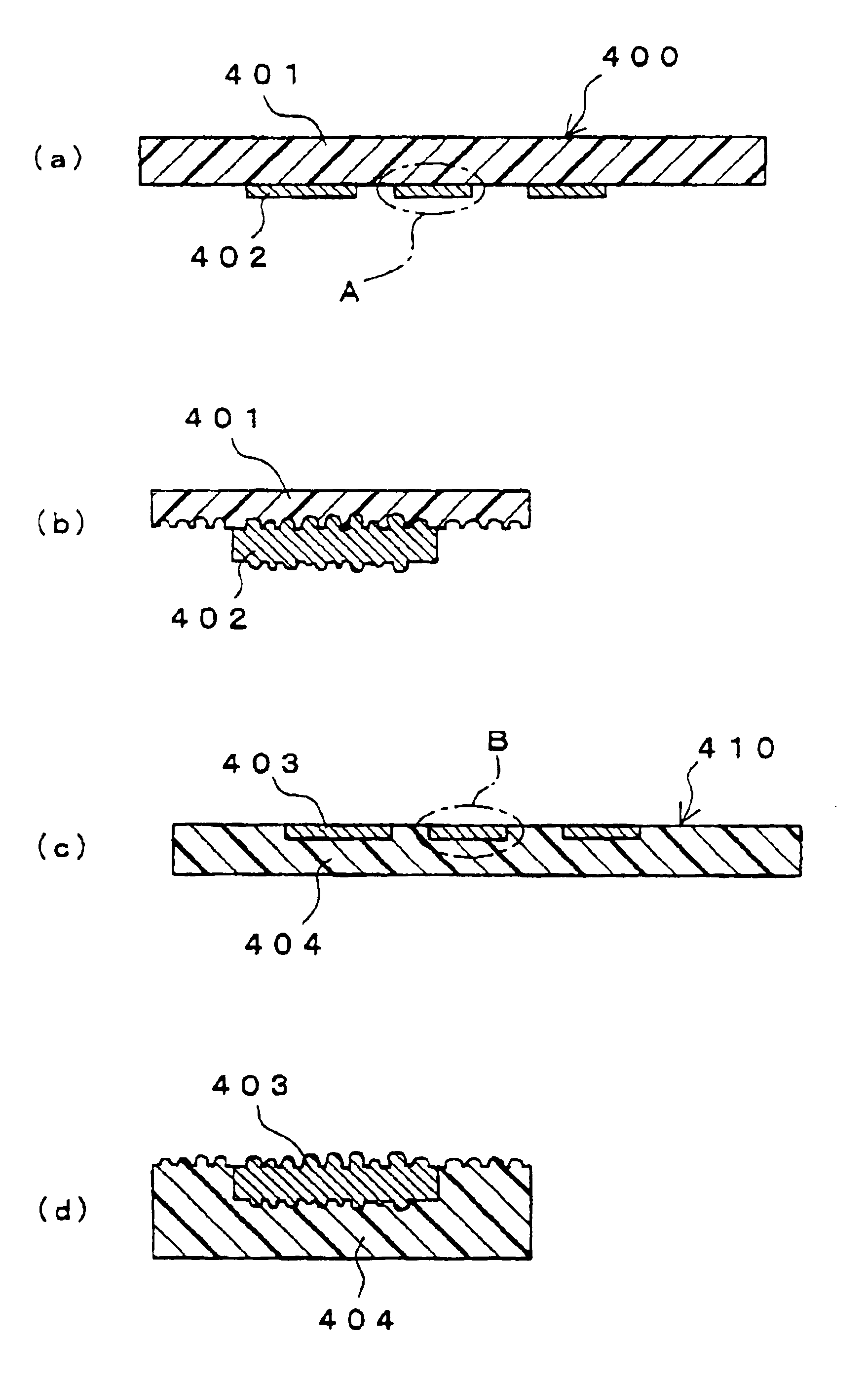
[0112]In FIG. 1, a wiring transfer sheet of Embodiment1 of the present invention and a wiring board which is produced using the wiring transfer sheet are schematically shown in sectional views. FIG. 1(a) shows a wiring transfer sheet 100 wherein a wiring layer 102 is formed in a predetermined pattern on a surface of a carrier base 101. FIG. 1(b) shows an enlarged view of Area B which is an exposed area of a surface of the carrier base is on which the wiring layer is formed. FIG. 1(c) shows an enlarged view of Area A in the vicinity of a the wiring layer of the wiring transfer sheet. FIG. 1(d) shows a wiring board 110 which is obtained by transferring a wiring layer 103 to an electrically insulating substrate 104 by using the wiring transfer sheet shown in FIG. 1(a). FIG. 1(e) shows an enlarged view of an Area D that is an exposed surface of the electrically insulating substrate, which is a part of a surface of the wiring board which surface has the wiring layer. FIG. 1...

embodiment 2

(Embodiment 2)

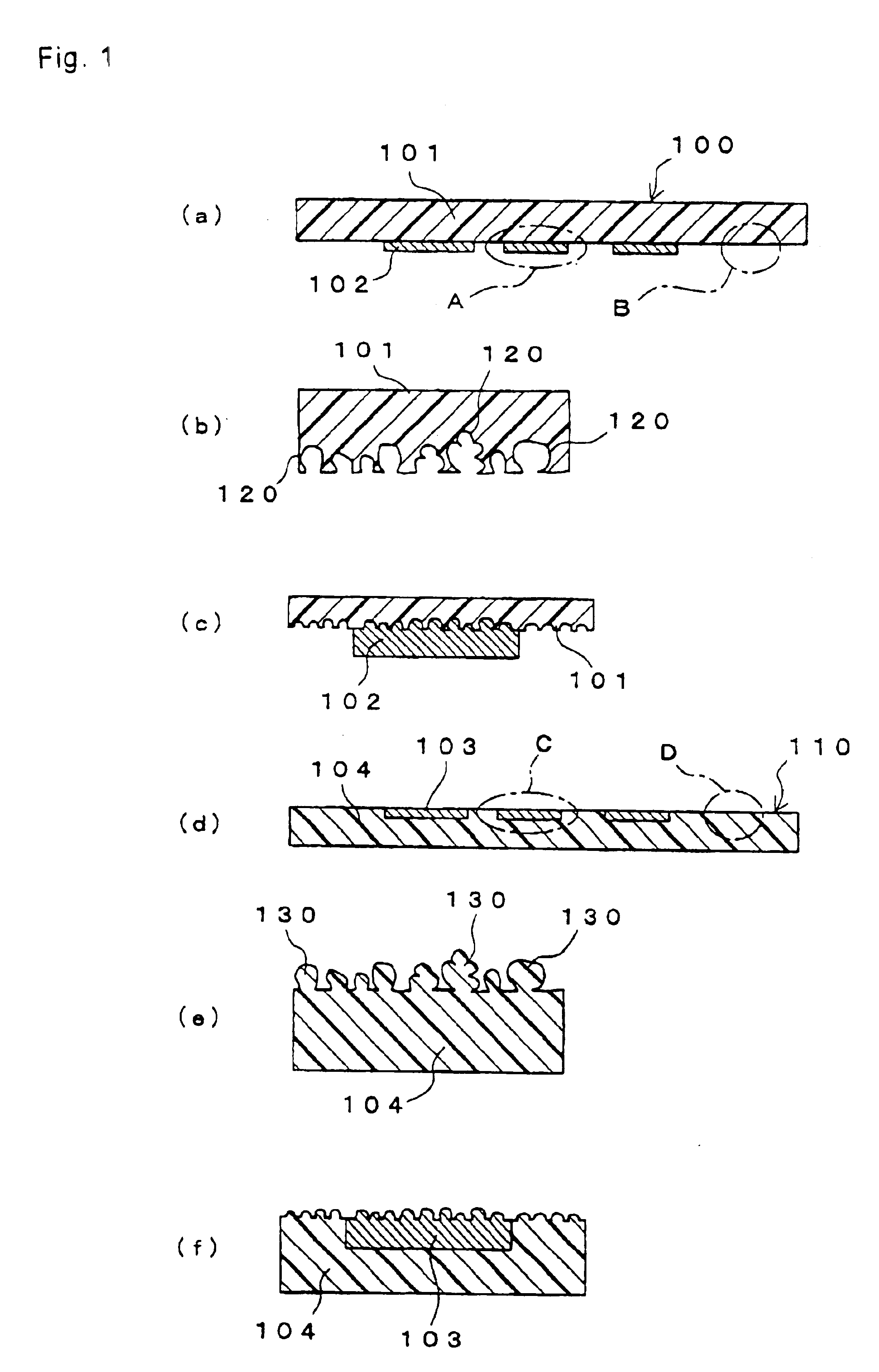
[0117]In FIG. 2, a wiring transfer sheet of Embodiment 2 of the present invention is schematically shown in sectional view. In a wiring transfer sheet 200 shown in FIG. 2, a carrier base 201 is formed of a wiring-forming layer 240 and a supporting layer 250, and a wiring layer 202 is formed on a surface of the wiring forming layer 240. In this wiring transfer sheet 200, the concavities (not shown) are formed on an exposed surface of the wiring-forming layer. The materials suitable for constituting the wiring-forming layer 240 and the supporting layer 250 are as described above. More specifically, as a combination of supporting layer / wiring forming layer, a copper foil / a fluorine-containing resin is exemplified.

embodiment 3

(Embodiment 3)

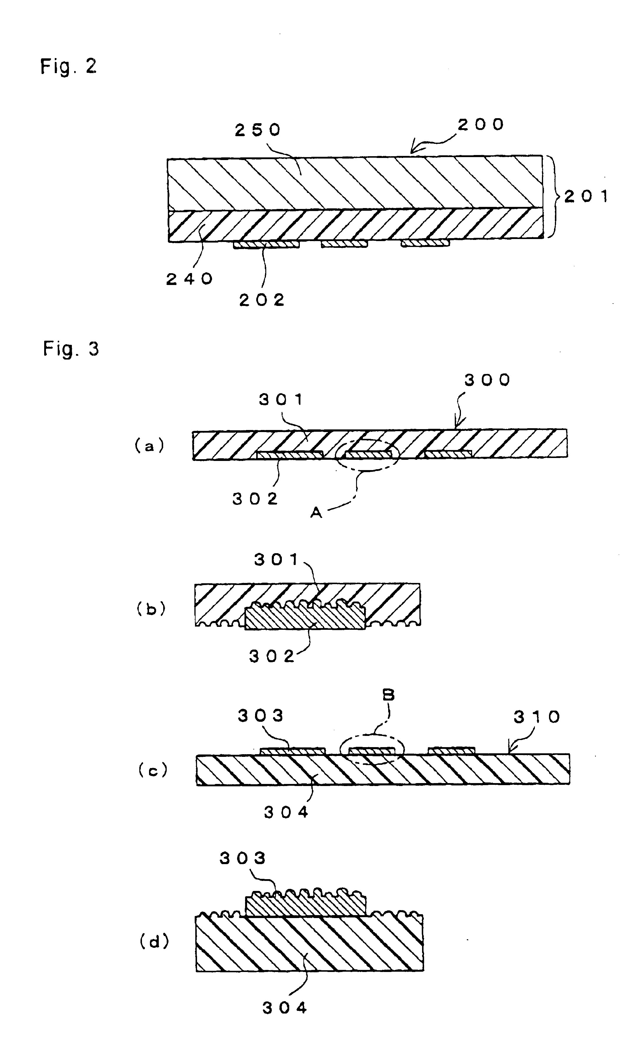
[0118]In FIG. 3, a wiring transfer sheet of Embodiment 3 of the present invention and a wiring board which is produced using the wiring transfer sheet are schematically shown in sectional views. FIG. 3(a) shows a wiring transfer sheet 300 wherein a wiring layer 302 is buried in a carrier base 301. FIG. 3(b) shows an enlarged view of Area A in the vicinity of the wiring layer of the wiring transfer sheet. FIG. 3(c) shows a wiring board 310 which is obtained by transferring a wiring layer 303 to an electrically insulating substrate 304 using the wiring transfer sheet shown in FIG. 3(a). FIG. 3(d) shows an enlarged view of Area B in the vicinity of the wiring layer of the wiring board.

[0119]As shown in FIG. 3(b), almost the entire thickness of the wiring layer 302 is buried in the carrier base 301 so that a surface of the wiring layer 302 is substantially flush with a surface of the carrier base 301. Such a wiring transfer sheet is produced by forming the wiring layer in ...


PUM

PropertyMeasurementUnit
diameteraaaaaaaaaa
heightaaaaaaaaaa
diameteraaaaaaaaaa

Abstract

A wiring transfer sheet including a carrier base and a wiring layer formed thereon is produced so that an exposed area of a surface of the carrier base on which the wiring layer is formed has a plurality of concavities. By transferring the wiring layer to an electrically insulating substrate with this wiring transfer sheet, convexities which are complementary to the concavities are formed on the electrically insulating substrate. The convexities improve adhesion between a wiring board and a resin stacked thereon. Therefore, the wiring board thus obtained has surface coplanarity suitable for mounting a semiconductor bare chip and an electronic component as a whole, and a microscopical surface structure which adheres to a material stacked thereon.

Description

[0001]This application is a Divisional Application of Ser. No. 10 / 420,876 filed Apr. 23, 2003 which is currently pending.CROSS-REFERENCE TO RELATED APPLICATIONS[0002]The present application claims a priority under 35 U.S.C. §119 to Japanese Patent Application No. 2002-124407 filed on Apr. 25, 2002, entitled “Wiring transfer sheet and method for producing the same, and wiring board and method for producing the same”. The contents of that application are incorporated herein by the reference thereto in their entirety.FIELD OF THE INVENTION[0003]The present invention relates to a wiring transfer sheet which is used for forming a wiring of a wiring board and to a method for producing the same, and further relates to a wiring board which is produced by using the wiring transfer sheet and a method for the wiring board by using the wiring transfer sheet.BACKGROUND OF THE INVENTION[0004]Recently, a multilayer wiring board on which semiconductor chips such as an LSI and so on can be mounted a...

Claims


Application Information

Patent Timeline
Patent Type & Authority Patents(United States)
IPC IPC(8): H05K3/20H05K3/46H05K3/38H05K3/40H05K3/06
CPCH05K1/187H05K3/20H05K3/381H05K3/382H05K3/4614H05K3/4617H05K3/462H01L2224/16Y10T428/2804H01L2924/01078H05K3/06H05K3/205H05K3/4069H05K3/4602H05K3/4652H05K3/4658H05K2201/10378H05K2203/0156H05K2203/061H05K2203/1152H01L2924/01087Y10S428/901Y10T29/49155Y10T428/12472Y10T428/12493Y10T29/49163Y10T428/12451Y10T428/24917Y10T29/49156Y10T29/49126Y10T428/12993H01L2924/01046Y10T428/249953
Inventor HIGASHITANI, HIDEKI
Owner PANASONIC CORP
Why Eureka
Try Eureka