Master information carrier for magnetic transfer
a master information and magnetic transfer technology, applied in the direction of soldering apparatus, instruments, manufacturing tools, etc., can solve the problems of deteriorating productivity, short time required for preformat recording, and greatly deteriorating quality of transferred signals, so as to improve the uniformity of magnetic fields in the area of transfer, improve the quality of reproduction signals, and improve the effect of slave medium
- Summary
- Abstract
- Description
- Claims
- Application Information
AI Technical Summary
Benefits of technology
Problems solved by technology
Method used
Image
Examples
examples
[0057]Master information carriers in accordance with first to eighth embodiments of the present invention and first to third comparative examples were made in the following way and the signal was transferred from the master information carriers to the slave media produced in the manner described later. Then transferred signal quality was evaluated in the following manner. The result is shown in the following table. In the table, “emb” is an abbreviation of “embodiment”, “c / e” is an abbreviation of “comparative example”, “CS” is an abbreviation of “crystallographic structure”, “ev” is an abbreviation of “evaluation”, and “ASY” is an abbreviation of “asymmetry”.
Evaluation of the Transferred Signal Quality
[0058]Quality of the signal reproduced from the slave medium was evaluated by the use of electromagnetic conversion property meter (SS-60: KYODO Electronics). A GMR head which was 0.12 μm in reproducing head gap, 0.41 μm in reproducing track width, 0.2 μm in recording head gap and 0.6...
first embodiment
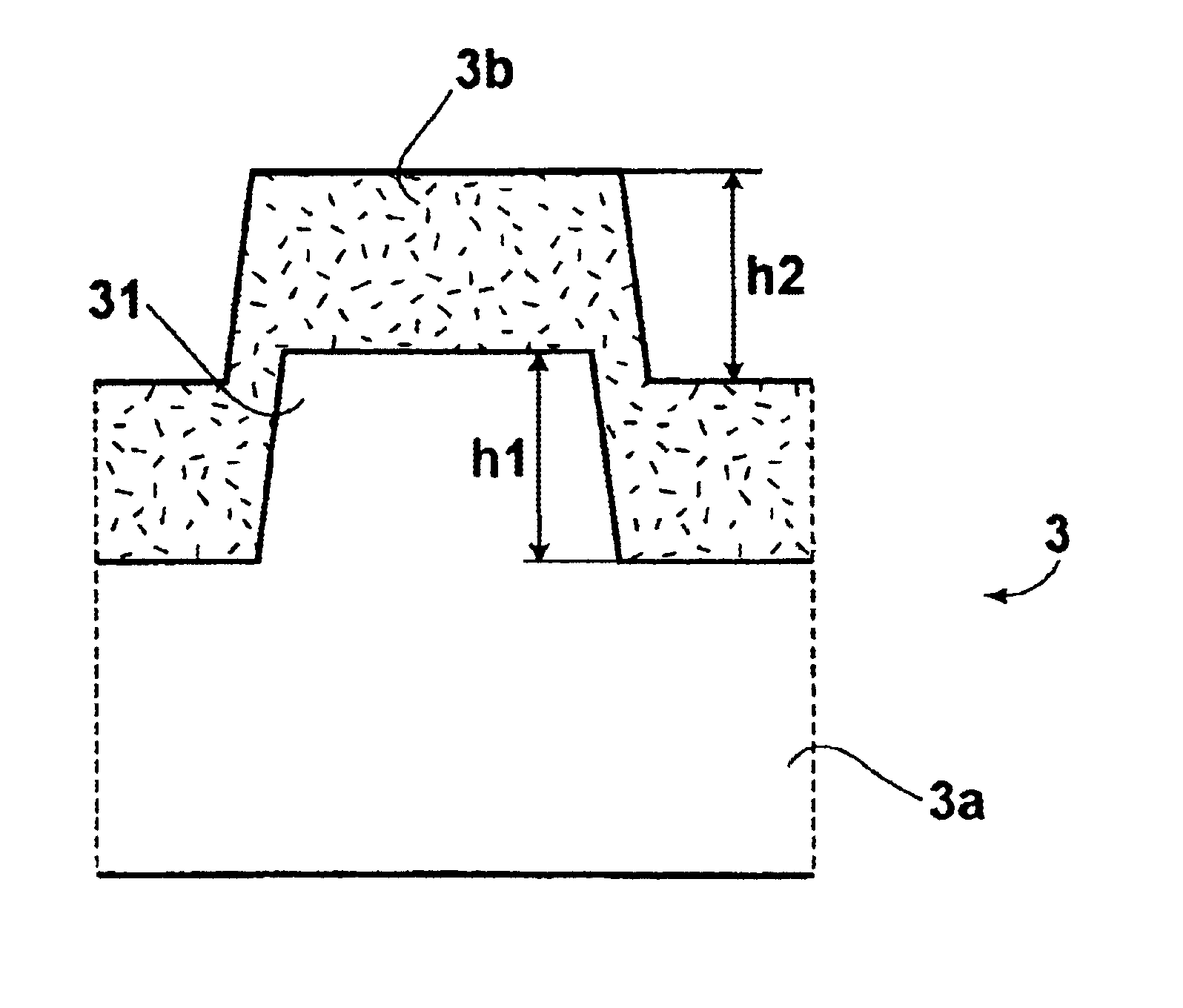
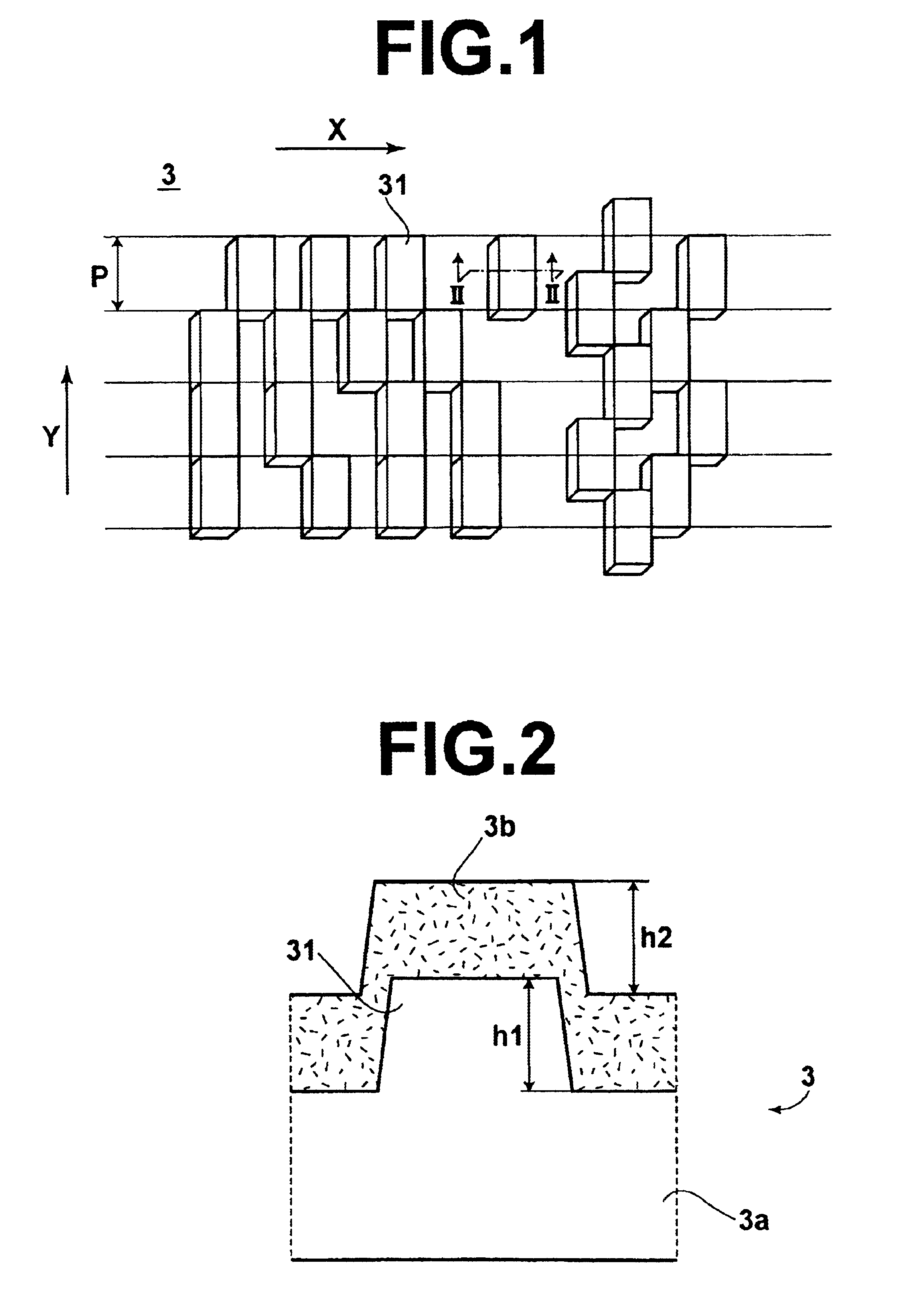
[0061]In the master information carrier in accordance with a first embodiment of the present invention, the base sheet was formed of Ni by the use of stamper method. An irregularity pattern signal which were 1.0 μm in track width and 1.1 μm in track pitch and extended from an innermost position at a distance of 20 mm from the center to an outermost position at a distance of 40 mm from the center was formed on the base sheet in a height of 0.2 μm of the protruding portions. The bit length was 0.2 μm in the innermost position.
[0062]A magnetic layer of FeCO (30 at %) having a bcc structure was formed on the Ni base sheet at 25° C. The Ar sputtering pressure was 1.44×10⁻¹ Pa (1.08 mTorr), and the power supplied was 2.80 W / cm2.
[0063]In the master information carrier of the first embodiment, Mm / Ms=3.8 and h2 / h1=0.7.
[0064]The master information carriers of the second to eighth embodiments and the first to third comparative examples were produced in manners similar to the first embodiment e...
second embodiment
[0065]The master information carrier of the second embodiment was produced in the same manner as the first embodiment except that the magnetic layer was of Co having a hcp structure and Mm / Ms was 2.8.
PUM
| Property | Measurement | Unit |
|---|---|---|
| height | aaaaa | aaaaa |
| size | aaaaa | aaaaa |
| height h1 | aaaaa | aaaaa |
Abstract
Description
Claims
Application Information
 - R&D
- Intellectual Property
- Life Sciences
- Materials
- Tech Scout
- Unparalleled Data Quality
- Higher Quality Content
- 60% Fewer Hallucinations
Browse by: Latest US Patents, China's latest patents, Technical Efficacy Thesaurus, Application Domain, Technology Topic, Popular Technical Reports.
© 2025 PatSnap. All rights reserved.Legal|Privacy policy|Modern Slavery Act Transparency Statement|Sitemap|About US| Contact US: help@patsnap.com


