Lithographic projection apparatus with multiple suppression meshes

a technology of lithographic projection apparatus and mesh, which is applied in the field of lithography, can solve the problems of high power consumption of the mesh, xe gas absorbs euv radiation, and attracts free electrons to the mesh, and achieves the effect of condensing the electric field

Inactive Publication Date: 2005-06-14
ASML NETHERLANDS BV
View PDF3 Cites 17 Cited by
  • Summary
  • Abstract
  • Description
  • Claims
  • Application Information

AI Technical Summary

Benefits of technology

[0015]At least one aspect of embodiments of the present invention is directed to reduce the number of free electrons that reach the high voltage mesh, and to confine the electric field.

Problems solved by technology

A drawback of such a rather high Xe pressure is that Xe gas absorbs EUV radiation.
However, the high positive voltage attracts free electrons to the mesh.
This results in several disadvantages such as: high power consumption in the mesh and the resulting heating of the mesh and the need for large high voltage power supplies for the mesh and the possibility of a gas discharge in the vicinity of the mesh.
Furthermore, the accompanying extending electric field results in electrical breakdown of the gas between the mesh and another surface and has a negative influence on the EUV source performance in the lithographic projection apparatus.

Method used


Image

  • Lithographic projection apparatus with multiple suppression meshes
  • Lithographic projection apparatus with multiple suppression meshes
  • Lithographic projection apparatus with multiple suppression meshes

Examples


Embodiment Construction

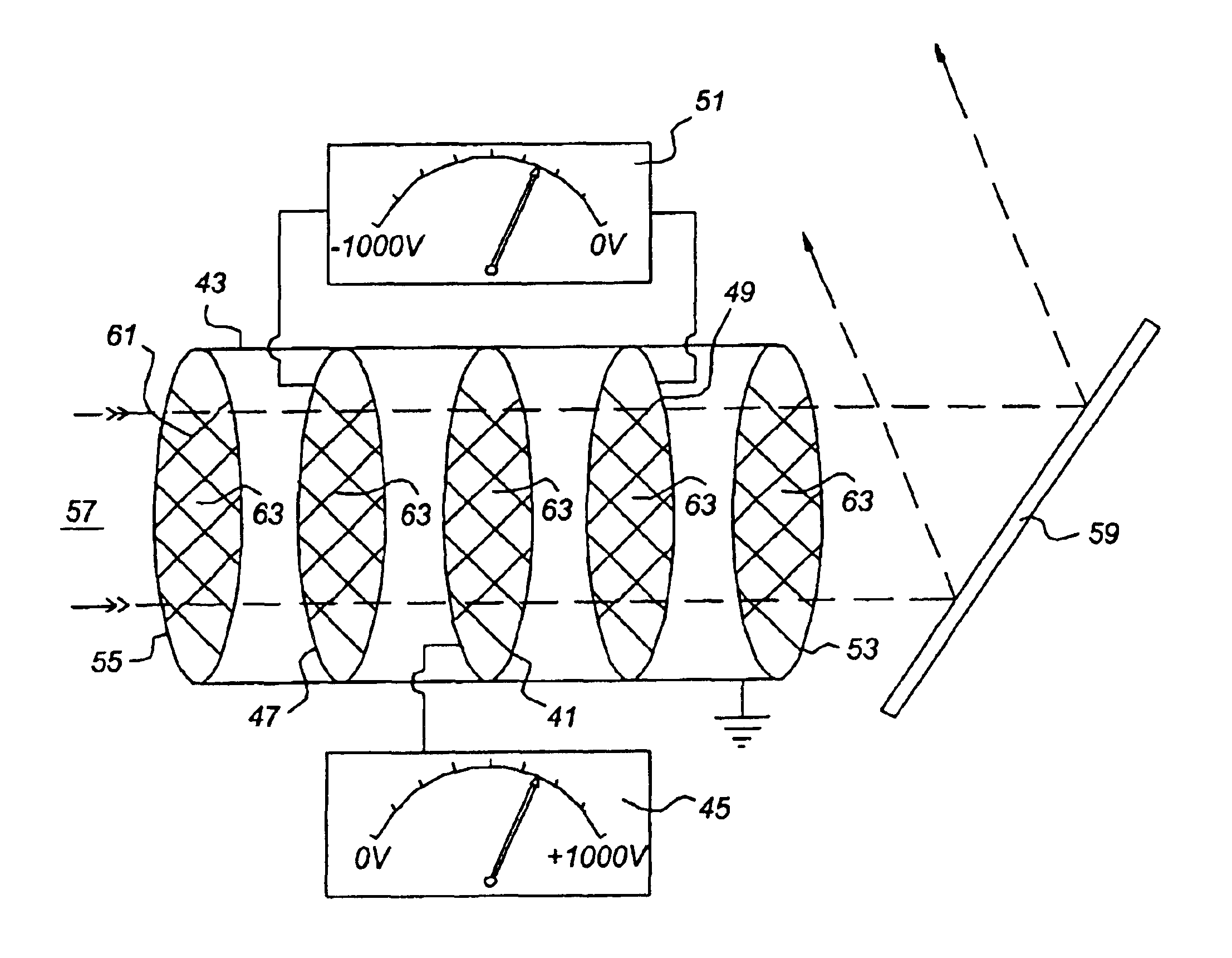
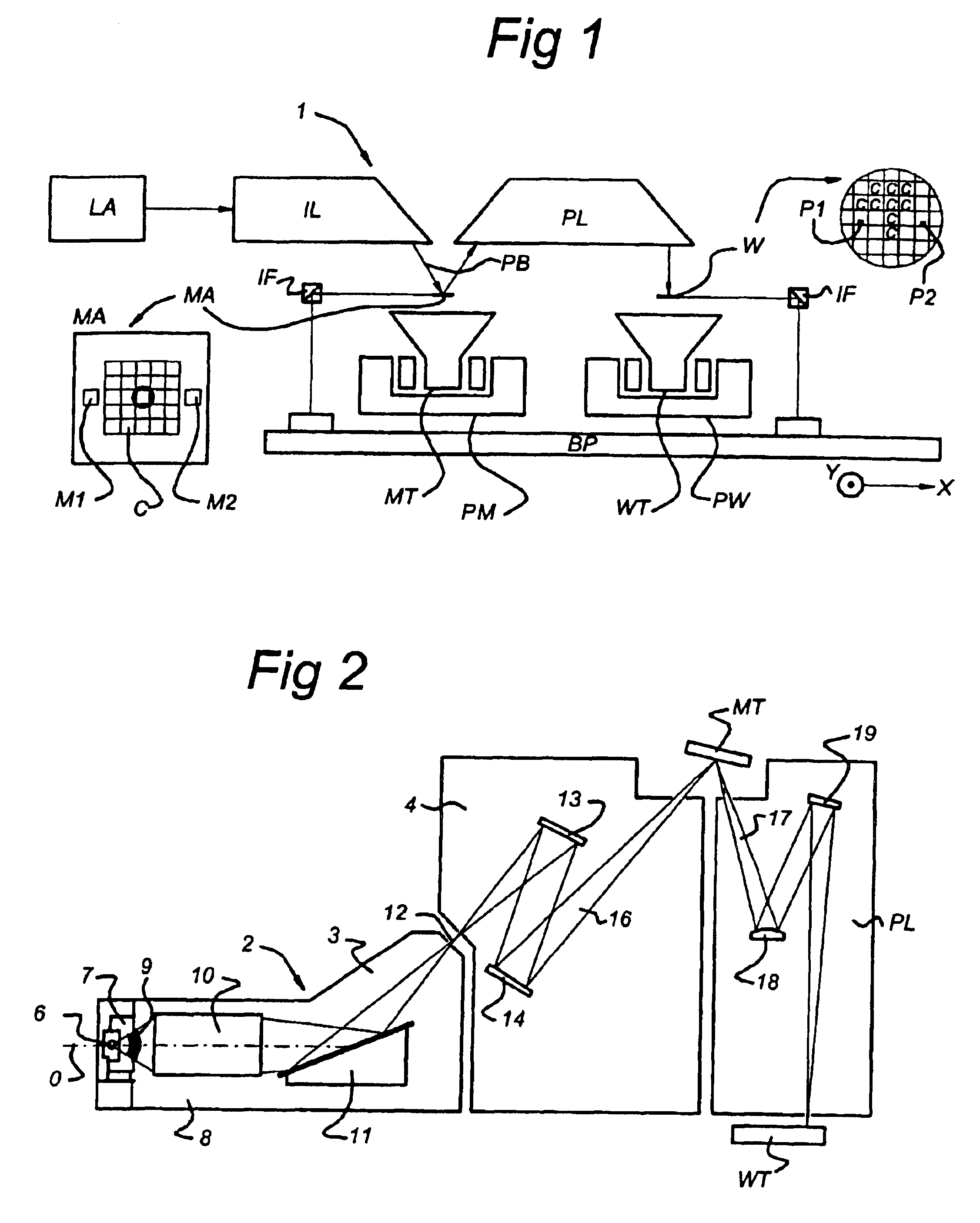
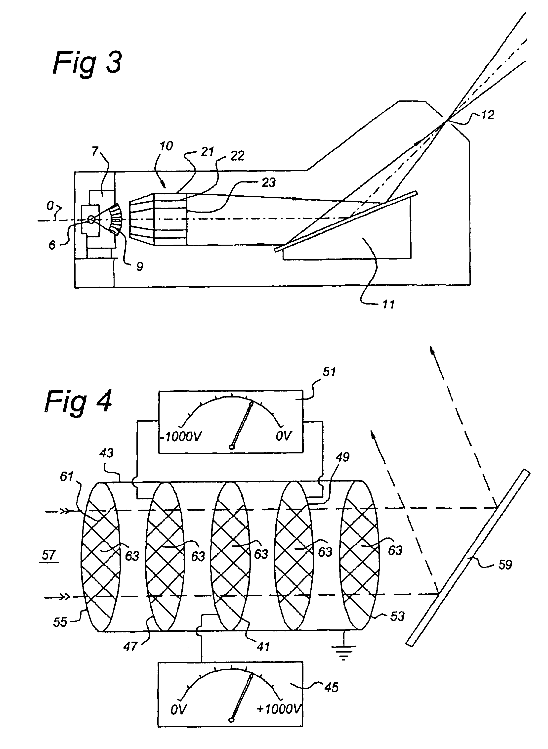
[0036]FIG. 1 schematically depicts a lithographic projection apparatus 1 according to a particular embodiment of the invention. The apparatus comprises a radiation system for supplying a projection beam PB of radiation (e.g. EUV radiation with a wavelength of 11-nm), a first object table (mask table) MT provided with a mask holder for holding a mask MA (e.g. a reticle), and connected to first positioning means PM for accurately positioning the mask with respect to item PL, a second object table (substrate table) WT provided with a substrate holder for holding a substrate W (e.g. a resist coated silicon wafer), and connected to second positioning means PW for accurately positioning the substrate with respect to item PL, and a projection system (“lens”) PL for imaging an irradiated portion of the mask MA onto a target portion C (e.g. comprising one or more dies) of the substrate W. In this particular case, the radiation system also comprises a radiation source LA. The term mask table ...


PUM

PropertyMeasurementUnit
positive voltageaaaaaaaaaa

Abstract

A lithographic projection apparatus is disclosed. The apparatus includes a radiation system to transmit a beam of radiation emitted from a radiation source, and a support structure constructed to hold a patterning structure to be irradiated by the beam. A substrate holder is constructed to hold a substrate, and a projection system is constructed and arranged to project an irradiated portion of the patterning structure onto a target portion of the substrate. A first screen is positioned in a path of the beam between the radiation system and an optical element and a positive voltage is applied to the first screen to repel positively charged particles away from the optical element. A second screen is positioned in the path of the beam on at least one side of the first screen, and a negative voltage is applied to the second screen to repel negative particles away from the first screen.

Description

CROSS-REFERENCE TO RELATED APPLICATIONS[0001]This application is based on and claims priority from European Patent Application No. 02079864.1 filed on Nov. 22, 2002, the contents of which are incorporated herein by reference.BACKGROUND OF THE INVENTION[0002]1. Field of the Invention[0003]The present invention relates generally to the field of lithography. More specifically, the present invention relates to a screen for an optical element.[0004]2. Description of Related Art[0005]The term “patterning device” or “patterning structure” as here employed should be broadly interpreted as referring to means or structure that can be used to endow an incoming radiation beam with a patterned cross-section, corresponding to a pattern that is to be created in a target portion of the substrate; the term “light valve” can also be used in this context. Generally, the pattern will correspond to a particular functional layer in a device being created in the target portion, such as an integrated circu...

Claims


Application Information

Patent Timeline
Patent Type & Authority Patents(United States)
IPC IPC(8): G03F7/20G21K5/00G21K5/02G21K3/00H01L21/027H05G2/00
CPCG03F7/70916G03F7/70983G03F7/70941G03F7/20
Inventor BAKKER, LEVINUS PIETERSCHUURMANS, FRANK JEROEN PIETER
Owner ASML NETHERLANDS BV
Why Eureka
Try Eureka