
Method of fabrication of thin film resistor with zero TCR

a thin film resistor and fabrication method technology, applied in resistors, semiconductor devices, solid-state devices, etc., can solve the problems of affecting the performance of high-performance semiconductor ic devices, resistance fluctuation hampering the performance of high-performance semiconductor devices, and the prior art resistor comprised of doped polysilicon can only provide a limited resistance within a limited space, so as to preserve the morphology of the upper resistor material and reduce the interfacial resistance

Inactive Publication Date: 2005-05-10
IBM CORP
View PDF6 Cites 52 Cited by
  • Summary
  • Abstract
  • Description
  • Claims
  • Application Information

AI Technical Summary

Benefits of technology

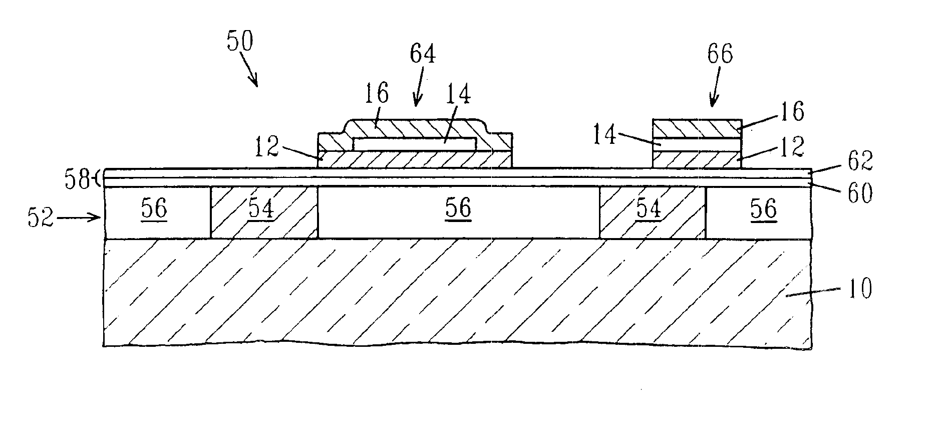
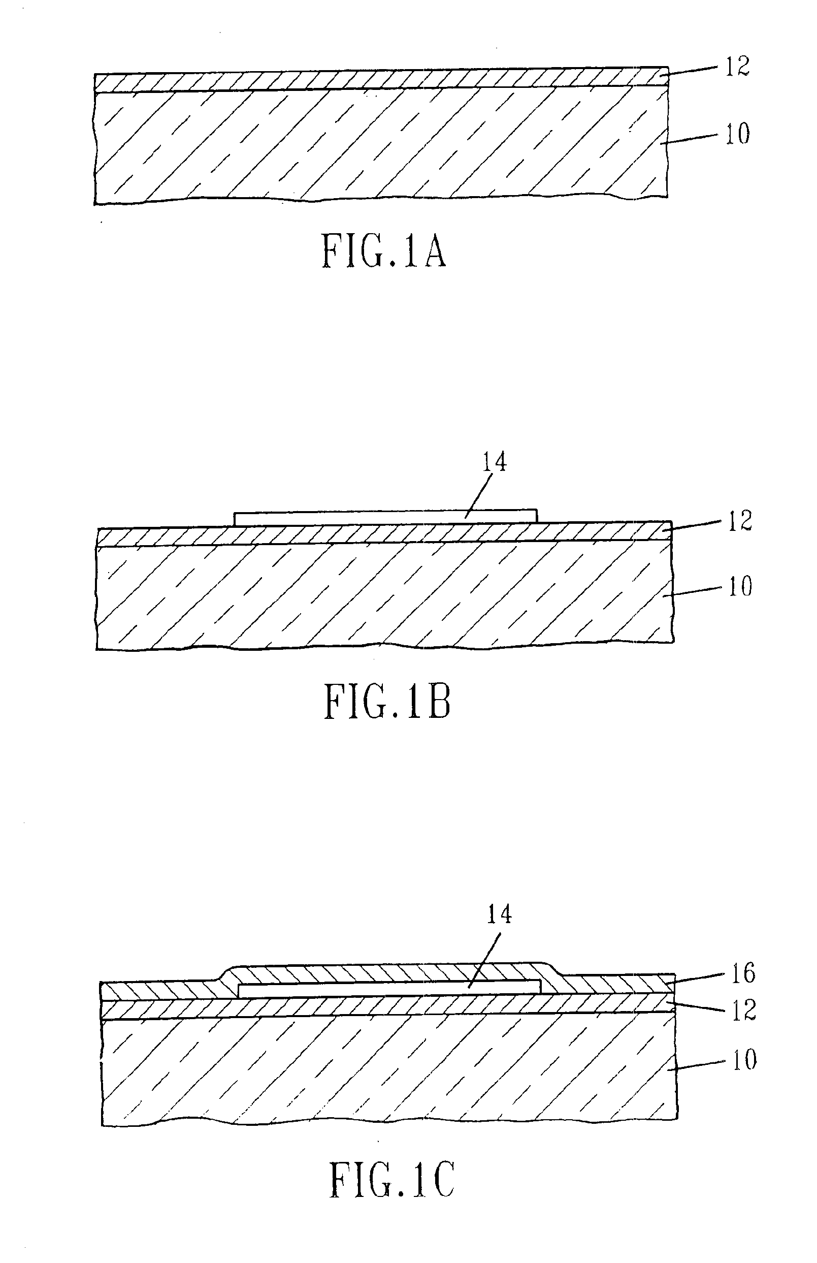
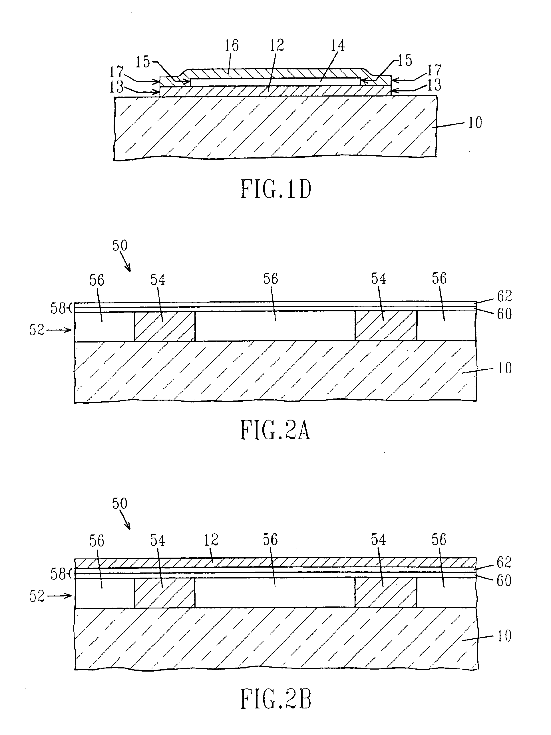
[0017]A selected and targeted sheet resistance can be provided to the thin film resistor of the present invention by selecting appropriate resistor materials that have a sheet resistance that provides the selected and targeted value. The thin film resistor of the present invention may include an insulating material located between portions of the resistor materials in which the outermost edges of the insulating material does not extend beyond the outermost edges of the at least two resistor materials. The insulating material is used in the present invention to reduce the interfacial resistance between overlying resistor materials as well as to preserve the morphology of the upper resistor material.

Problems solved by technology

However, due to the properties of polysilicon, a prior art resistor comprised of doped polysilicon can only provide a limited resistance within a limited space.
Employing a polysilicon resistor to provide relatively high resistance then becomes a problem in designing and fabricating a highly integrated semiconductor device.
On account of the high TCR values of prior art single thin film resistors, the resistance of such resistors tends to fluctuate a lot when the resistor is used at normal operating temperatures of about 85° C.; resistance fluctuation hampers the performance of high-performance semiconductor IC devices.

Method used


Image

  • Method of fabrication of thin film resistor with zero TCR
  • Method of fabrication of thin film resistor with zero TCR
  • Method of fabrication of thin film resistor with zero TCR

Examples


Embodiment Construction

[0032]The present invention, which provides a thin film resistor having a substantially zero TCR, will now be described in greater detail by referring to the drawings that accompany the present application. In the accompanying drawings, like and corresponding elements are referred to by like reference numerals. Although the drawings show the presence of two resistor materials, the present invention is not limited to resistors having only two layers. Instead, the present invention works equally well in forming a plurality of resistor materials, one over the other, in which the TCR value of the various resistor material layers is substantially zero TCR.

[0033]As stated above, the present invention provides a thin film resistor that has a substantially zero TCR. The thin film resistor of the present invention includes at least two resistor materials located over one another. Each resistor material has a different temperature coefficient of resistivity which provides an effective tempera...


PUM


Abstract

A thin film resistor that has a substantially zero TCR is provided as well as a method for fabricating the same. The thin film resistor includes at least two resistor materials located over one another. Each resistor material has a different temperature coefficient of resistivity such that the effective temperature coefficient of resistivity of the thin film resistor is substantially 0 ppm / ° C. The thin film resistor may be integrated into a interconnect structure or it may be integrated with a metal-insulator-metal capacitor (MIMCAP).

Description

RELATED APPLICATION[0001]This application is a divisional of U.S. application Ser. No. 10 / 250,075, filed Jun. 2, 2003.FIELD OF THE INVENTION[0002]The present invention relates to semiconductor device manufacturing, and more particularly to a method of fabricating a thin film resistor having a substantially zero “0” temperature coefficient of resistivity (TCR). The present invention is also directed to a method of integrating the thin film resistor of the present invention with an interconnect structure and / or a metal-insulator-metal capacitor (MIMCAP).BACKGROUND OF THE INVENTION[0003]In semiconductor integrated circuits (ICs), a resistor may be used to control the resistance of other electronic components of the IC. As is known to those skilled in the art, the resistance, R, of a resistor is proportional to the length, L, of the resistor and the reciprocal cross sectional area, 1 / A, of the resistor; the L and A are measured in the direction of current flow. The basic equation for re...

Claims


Application Information

Patent Timeline
IPC IPC(8): H01C7/06H01C7/00
CPCH01C7/06H01C7/006
Inventor AMADON, JEFFREY R.CHINTHAKINDI, ANIL K.STEIN, KENNETH J.WONG, KWONG H.
Owner IBM CORP
Learn More