
Polymer compound for a chemical amplification resist and a fabrication process of a semiconductor device using such a chemical amplification resist

a technology of chemical amplification resist and polymer compound, which is applied in the direction of photosensitive materials, instruments, photomechanical devices, etc., can solve the problems of high cost of mevalonic lactone source material, strong optical absorption of resist, and inability to resist strong optical absorption

Inactive Publication Date: 2005-05-03
FUJITSU LTD
View PDF11 Cites 26 Cited by
  • Summary
  • Abstract
  • Description
  • Claims
  • Application Information

AI Technical Summary

Benefits of technology

The present invention provides a novel and useful resist composition that overcomes various problems associated with previous resist compositions. The resist composition includes a film-forming polymer with a carboxyl group and an additional acidic functional group that has an acid-cleavable protective group. The polymer has high sensitivity to deep-ultraviolet optical radiation and has excellent dry-etching resistance. The resist composition is insoluble to a basic solution but becomes soluble after exposure to an optical radiation. The composition can form ultra-fine patterns with high resolution and sharp contrast. The resist composition is suitable for use in the fabrication of semiconductor devices using a deep-ultraviolet laser as the light source. The composition has an optical absorption of 1.75 or less in the deep-ultraviolet wavelength band of 180-300 nm. The composition can be supplied in a solution dissolved into a solvent.

Problems solved by technology

In the photolithographic process that uses such a very short wavelength optical radiation, the problem of strong optical absorption by the resist is inevitable as long as a phenolic polymer resin is used for the resist base.
On the other hand, the foregoing conventional resists have suffered from the problems, associated with the use of the alicyclic group in the resin,such as a peeling-off of the resist during the developing process or an insufficient dissolving of the exposed area to an alkaline developer.
On the other hand, there has been a problem in the foregoing conventional resist composition in that the synthesis of mevalonic lactone methacrylate has to be conducted at a low temperature, and that the mevalonic lactone source material is expensive.

Method used


Image

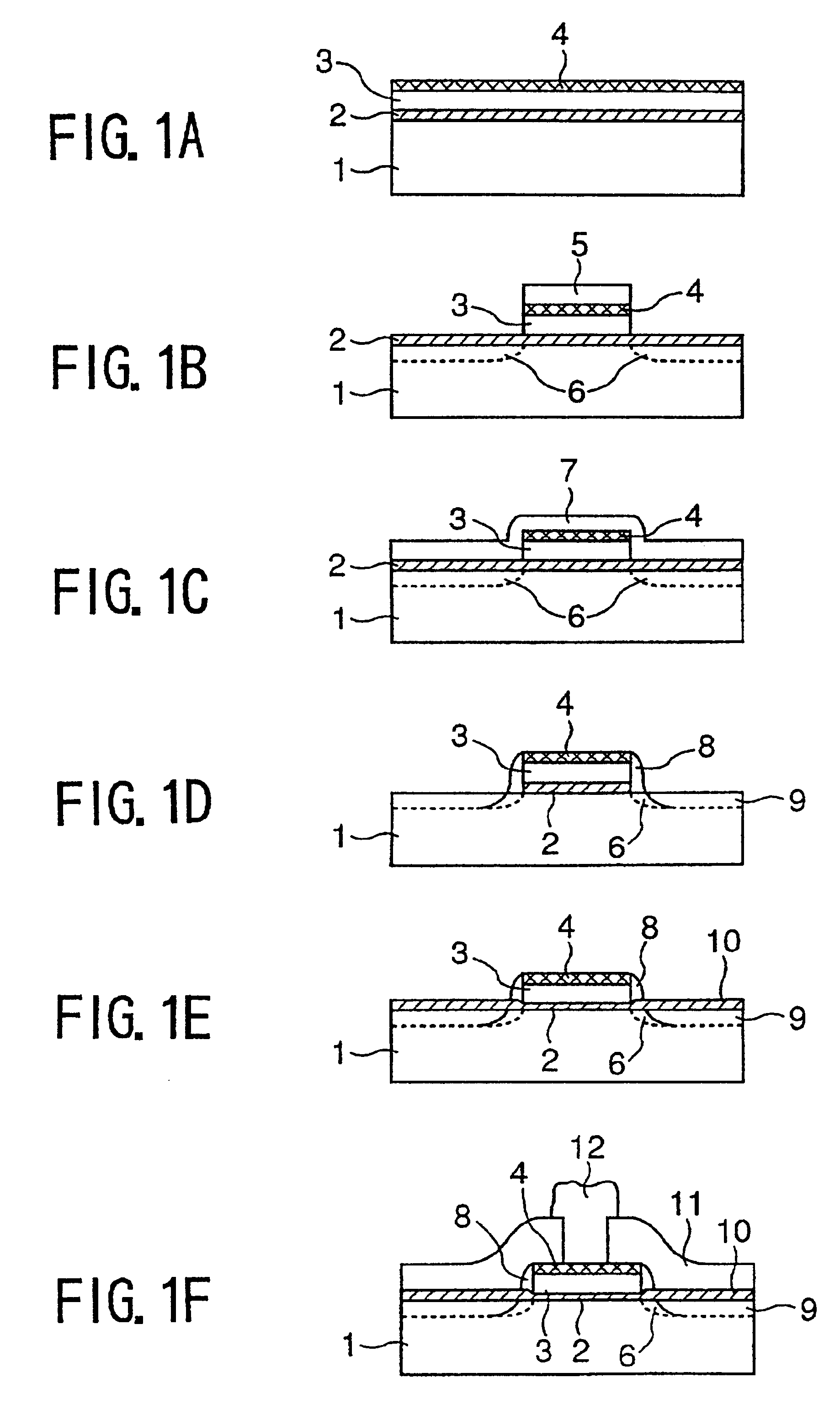
  • Polymer compound for a chemical amplification resist and a fabrication process of a semiconductor device using such a chemical amplification resist
  • Polymer compound for a chemical amplification resist and a fabrication process of a semiconductor device using such a chemical amplification resist
  • Polymer compound for a chemical amplification resist and a fabrication process of a semiconductor device using such a chemical amplification resist

Examples


first embodiment

Synthesis of γ-Butylolactone-2-yl Methacrylate

[0077]A three-neck flask of 200 ml size is dried thoroughly and filled with N2, after connecting thereto a dropping funnel, a calcium chloride tube and a N2 supply tube at respective necks. Next, 50 ml of dry methylene chloride, 5.0 g (48.9 mmol) of 2-hydroxy-γ(gamma)-butylolactone, and 5.45 g (53.9 mmol) of dry triethylamine are introduced into the three-neck flask and stirred in an N2 atmosphere at 0° C. by using a teflon-coated stirrer bar.

[0078]Next, 5.11 g (48.9 mmol) of methacryloyl chloride previously held in the dropping funnel is introduced by a dropping process conducted for 1 hour, and the liquid thus obtained is stirred at a room temperature for 2 hours. The resultant solution is then taken into a separating funnel of a 300 ml size, and the solution thus taken is washed with 100 ml of water, followed by washing with a saturated sodium chloride water. Thereby, the water layer is extracted three times with methylene chloride, a...

second embodiment

Synthesis of a Copolymer of γ-Butylolactone-2-yl Methacrylate and 2-Methyl-2-Adamantyl Methacrylate

[0081]A flask of 100 ml size is used to hold 3 g (17.6 mmol) of γ(gamma)-butylolactone-2-yl methacrylate, 3.51 g (14.4 mmol) of 2-methyl-2-adamantyl methacrylate, 788 mg (4.8mmol) of AIBM (15 mol %) and 10.7 ml of dioxane, together with a magnetic stirrer bar, and the mixture in the flask is stirred by using the magnetic stirrer bar in a dry N2 environment at a temperature of 70° C. for 8 hours. A resultant viscous fluid is added dropwise in 800 ml of methanol, to form a precipitate.

[0082]Next, the precipitate is filtered by using a glass filter and the resin thus filtered is dried in a vacuum oven at 45° C. for 6 hours. The resin thus obtained is then dissolved into THF. After repeating the precipitation purification twice by using methanol, the resin is dried in the vacuum oven at 45° C. for 18 hours. As a result, a whitish resin powder is obtained with a yield of 5.35 g (82.2%).

[008...

third embodiment

Resist Pattern Formation

[0087]The copolymer synthesized in the second embodiment is dissolved into PGMEA (propyleneglycol methylether acetate) to form a 15 wt % solution. The solution is further added with 8 wt % γ(gamma)-butylolactone as the auxiliary solvent. The solution thus obtained is further added with 2 wt % of triphenylsulfonium trifluorosulfonate for complete dissolution.

[0088]The resist solution thus obtained is then filtered by a teflon membrane filter of 0.2 μm size and spun onto a Si substrate processed by HMDS, to form a resist film. The resist film thus formed is subjected to a prebaking process at 120° C. for 60 seconds, and a resist film having a thickness of 0.7 μm.

[0089]The resist film thus obtained is then subjected to an exposure process, in which the exposure process is conducted by a KrF excimer laser stepper having a numerical aperture of 0.45.

[0090]After the exposure, the resist film is subjected to a PEB process at a temperature of 110° C. for 60 seconds, ...


PUM

PropertyMeasurementUnit
thicknessaaaaaaaaaa
widthaaaaaaaaaa
wavelengthaaaaaaaaaa

Abstract

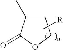
A resist composition includes a polymer principal chain, a carboxyl group having a protective group and bonding to a side chain of the polymer main chain, and an additional acidic functional group having an acid-cleavable protective group and bonding to a side chain of the polymer main chain, wherein the carboxyl group has a lactone structure represented by a formula (wherein n is an integer of 1-4, and R represents any of a hydrogen atom, an alkyl group, an alkoxyl group and an alkoxycarbonyl group and connected to an arbitrary position of said lactone structure excluding a second position forming an ester bonding) as the protective group.

Description

BACKGROUND OF THE INVENTION[0001]The present invention generally relates to a resist composition that can be developed by a basic developing liquid and a fabrication process of a semiconductor device using such a resist composition.[0002]With the advancement in the art of device miniaturization, recent semiconductor integrated circuits designated as LSIs or VLSIs are now patterned with sub-micron line widths. Further, intensive investigations are being made on so-called sub-halfmicron devices that use a minimum pattern width of smaller than 0.5 μm.[0003]In order to fabricate such sub-halfmicron devices, it is essential to reduce the wavelength of the optical radiation that is used for exposing a pattern on a semiconductor substrate, from a conventional, normal ultraviolet wavelength to a far-ultraviolet wavelength. Further, investigations are being made also on the exposure process that uses a deep ultraviolet wavelength radiation. Associated with such a shift in the wavelength of t...

Claims


Application Information

Patent Timeline
Patent Type & Authority Patents(United States)
IPC IPC(8): C08F12/00C08F20/00C08F12/04C08F20/26C08F246/00C08F22/00C08F22/40G03F7/30G03F7/40G03F1/00G03F7/039G03F7/004G03F7/033H01L21/02H01L21/027H01L21/3065C08F220/18C08F220/28H01L21/302
CPCG03F7/0392G03F7/0397Y10S430/111Y10S430/106G03F7/00G03F7/004
Inventor NOZAKI, KOJIYANO, EI
Owner FUJITSU LTD
Learn More