Semiconductor device and manufacturing method thereof
a technology of semiconductor devices and manufacturing methods, applied in semiconductor devices, semiconductor/solid-state device details, electrical apparatus, etc., can solve the problems of increasing the assembling steps to raise the material cost and assembly cost, and increasing the thickness of the whole package, so as to reduce the thickness, reduce the manufacturing process, and the effect of high-density mounting
- Summary
- Abstract
- Description
- Claims
- Application Information
AI Technical Summary
Benefits of technology
Problems solved by technology
Method used
Image

Examples
first embodiment
(Structure)
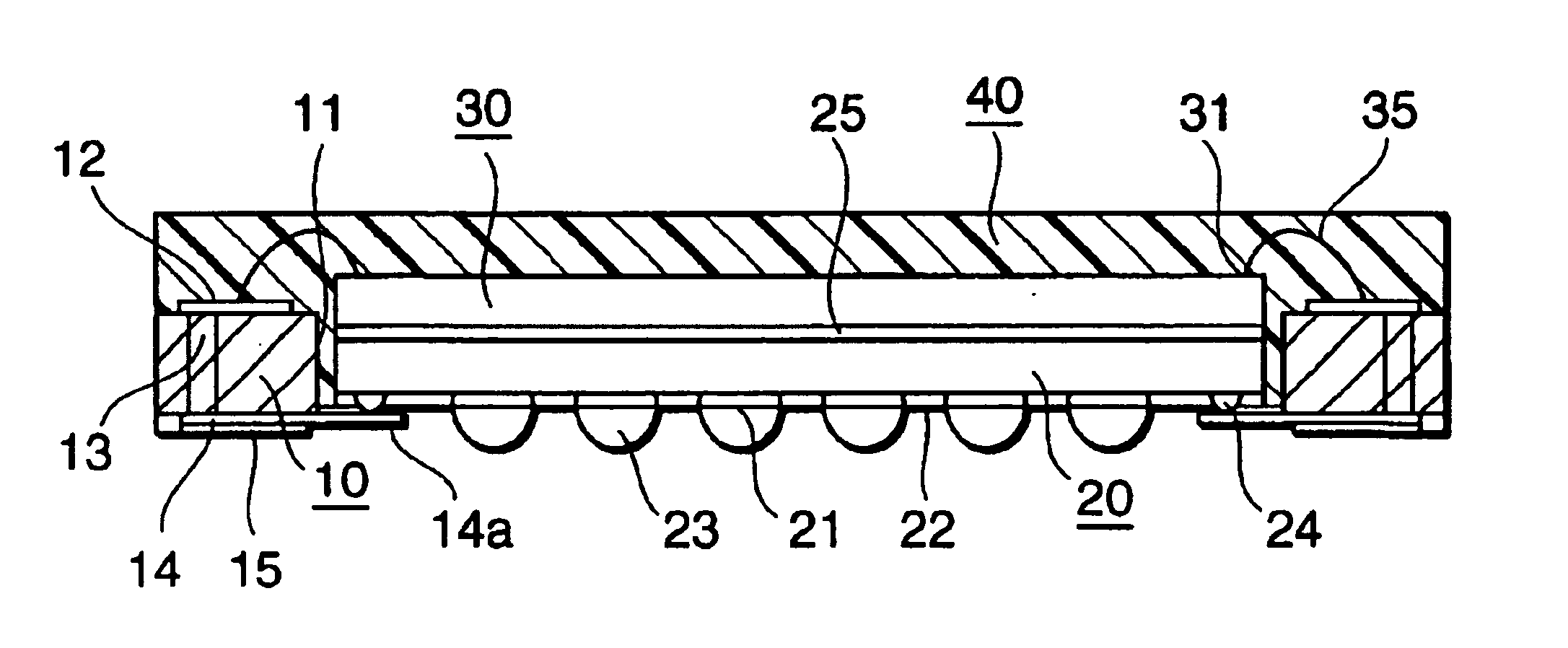
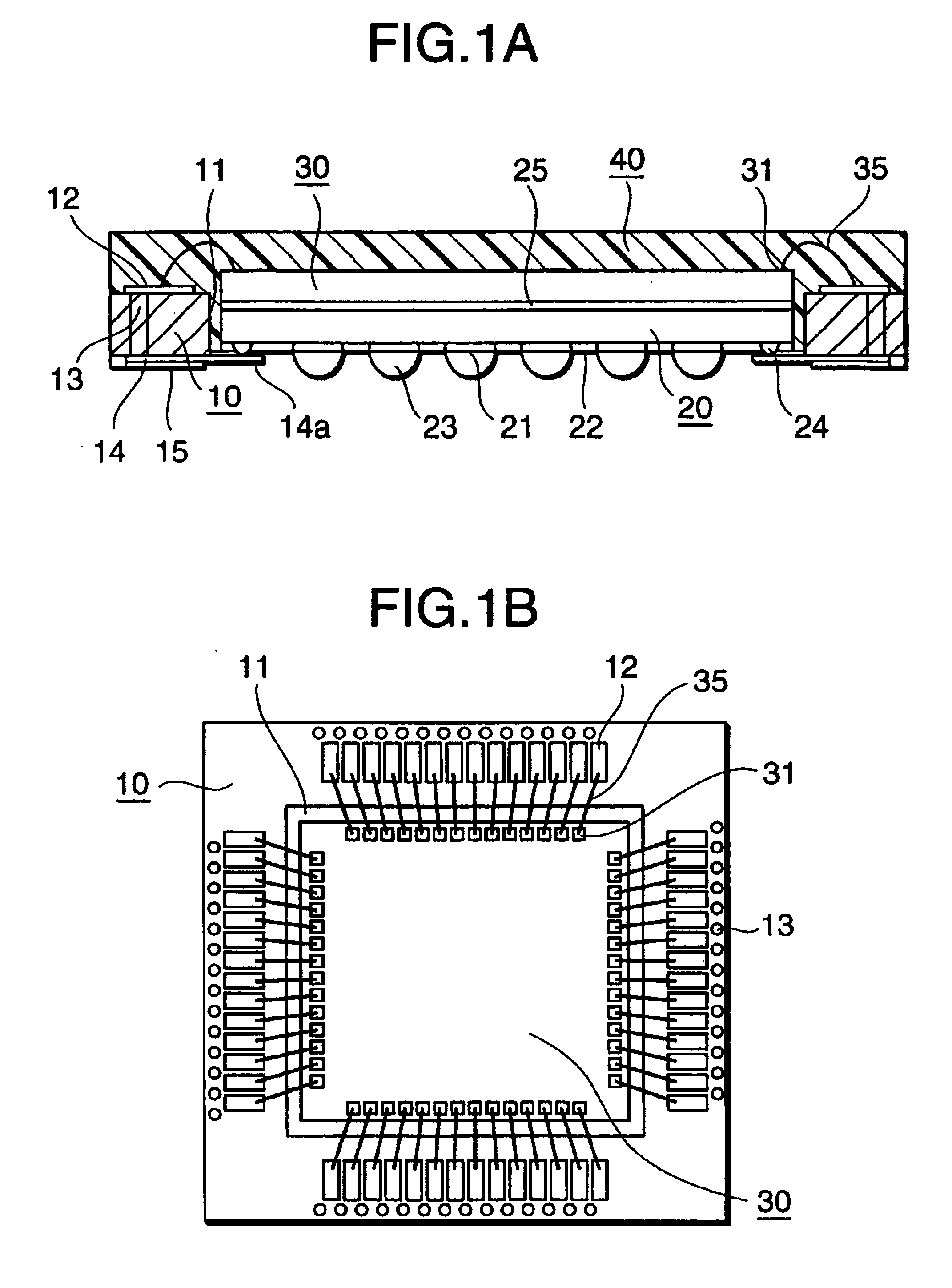
FIGS. 1A and 1B are structural diagrams of a semiconductor device showing a first embodiment of the present invention, wherein FIG. 1A is an enlarged sectional view and FIG. 1B is a plan view before sealing. FIGS. 2A and 2B are structural diagrams of the semiconductor device, wherein FIG. 2A is a bottom view of the semiconductor device and FIG. 2B is a plan view of a first chip in the semiconductor device.
This semiconductor device, for example, has a fine pitch ball grid alley (hereinafter referred to as “FBGA”) structure with a pitch of 0.8 mm or less in an equal-chip-size two-chip stacked MCP structure, and comprises a wiring substrate 10 in the form of a glass epoxy substrate, a polyimide substrate, or the like. At a predetermined portion of the wiring substrate 10, there is formed an opening portion 11 having a predetermined shape (e.g. rectangular) and size and passing through the wiring substrate 10 from a first surface (e.g. front surface) thereof to a second surfa...
second embodiment
(Structure)
FIG. 3 is a bottom view of a semiconductor device showing a second embodiment of the present invention, wherein those elements common to the elements in FIGS. 1A, 1B, 2A and 2B showing the first embodiment are assigned the same reference symbols.
Like in the first embodiment, the semiconductor device in this embodiment has the FBGA structure in the equal-chip-size two-chip stacked MCP structure. This semiconductor device differs from the semiconductor device in the first embodiment in that inner end portions 14a of a plurality of wirings 14 projected into the opening portion 11 on the back surface side of the wiring substrate 10 are each formed round and large and are arranged zigzag so as to increase contact areas and, correspondingly, a plurality of internal connection terminals 24 formed on a front surface of a lower chip 20 are also arranged zigzag.
Like in the first embodiment, the wirings 14 are made of Cu or the like, and the inner end portions 14a thereof each proje...
third embodiment
(Structure etc.)
FIGS. 4A and 4B are structural diagrams of a semiconductor device showing a third embodiment of the present invention, wherein FIG. 4A is an enlarged sectional view, while FIG. 4B is a bottom view. In FIGS. 4A and 4B, those elements common to the elements in FIGS. 1A, 1B, 2A, 2B and 3 showing the first and second embodiments are assigned the same reference symbols.
Like in the first and second embodiments, the semiconductor device in this embodiment has the FBGA structure in the equal-chip-size two-chip stacked MCP structure. This semiconductor device differs from the semiconductor devices in the first and second embodiments in that, even if the front surface side of the wiring substrate 10 is sealed by the sealing body 40, the connecting portions between the inner end portions 14a of the wirings 14 and the internal connection terminals 24 are exposed, and thus, after the sealing by the sealing body 40, insulating members 41 such as liquid sealing resin are applied to...
PUM
 Abstract
Description
Claims
Application Information
 - R&D
- Intellectual Property
- Life Sciences
- Materials
- Tech Scout
- Unparalleled Data Quality
- Higher Quality Content
- 60% Fewer Hallucinations
Browse by: Latest US Patents, China's latest patents, Technical Efficacy Thesaurus, Application Domain, Technology Topic, Popular Technical Reports.
© 2025 PatSnap. All rights reserved.Legal|Privacy policy|Modern Slavery Act Transparency Statement|Sitemap|About US| Contact US: help@patsnap.com