Method of forming a metal wiring in a semiconductor device

a metal wiring and semiconductor technology, applied in semiconductor devices, semiconductor device details, electrical devices, etc., can solve the problems of increasing the leakage current, affecting the resistance, and preventing an increase in the via resistance. , to achieve the effect of facilitating partial filling and preventing an increase in the via resistan

Inactive Publication Date: 2004-04-20
SK HYNIX INC
View PDF12 Cites 1 Cited by
  • Summary
  • Abstract
  • Description
  • Claims
  • Application Information

AI Technical Summary

Benefits of technology

A metal wiring in a semiconductor device is disclosed that is capable of preventing an increase in the via resistance by forming a diffusion prevention film on the sidewall of a damascene pattern in the form of a spacer. The method also facilitates select partial filling of the damascene pattern using a copper precursor by selectively forming a chemical enhancer layer within the damascene pattern using a selective reaction property of the chemical enhancer.

Problems solved by technology

However, copper has a disadvantage that the diffusion speed of copper into a silicon oxide used as an insulating film in a semiconductor device is faster than aluminum.
Copper atoms that diffuse into the silicon oxide degrades transistors and capacitors in the semiconductor device and thus increase the leakage current.
Therefore, if a prevention barrier metal having a low resistivity is not suitably selected, it is thought that the effect of resistance will be great and dishing and erosion may be caused by the difference of a selective ratio with the diffusion barrier film during CMP process.
However, filling of copper using the CVD method has problems that the deposition speed is slow and the cost is high.
This method, however, has a problem in that the chemical enhancer must be uniformly sprayed and a selective filling method must be applied by which the chemical enhancer is distributed at a specific location, which is difficult to employ.

Method used


Image

  • Method of forming a metal wiring in a semiconductor device
  • Method of forming a metal wiring in a semiconductor device

Examples


Embodiment Construction

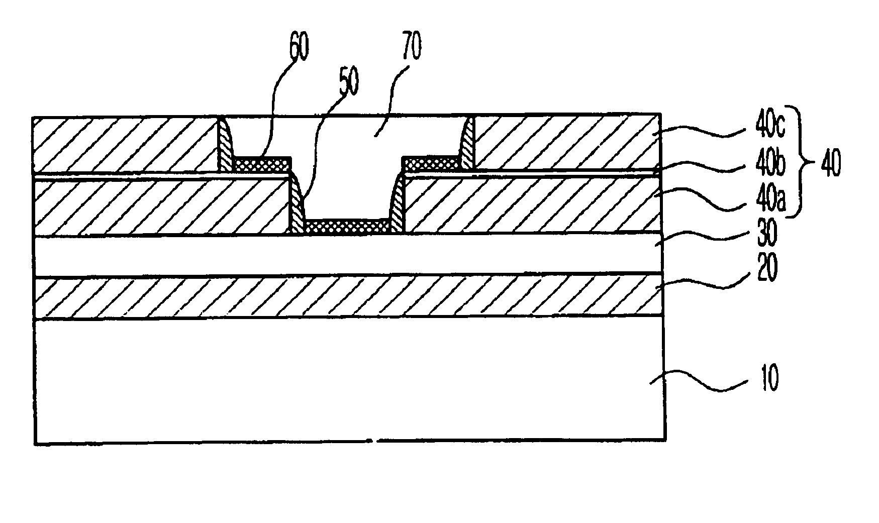
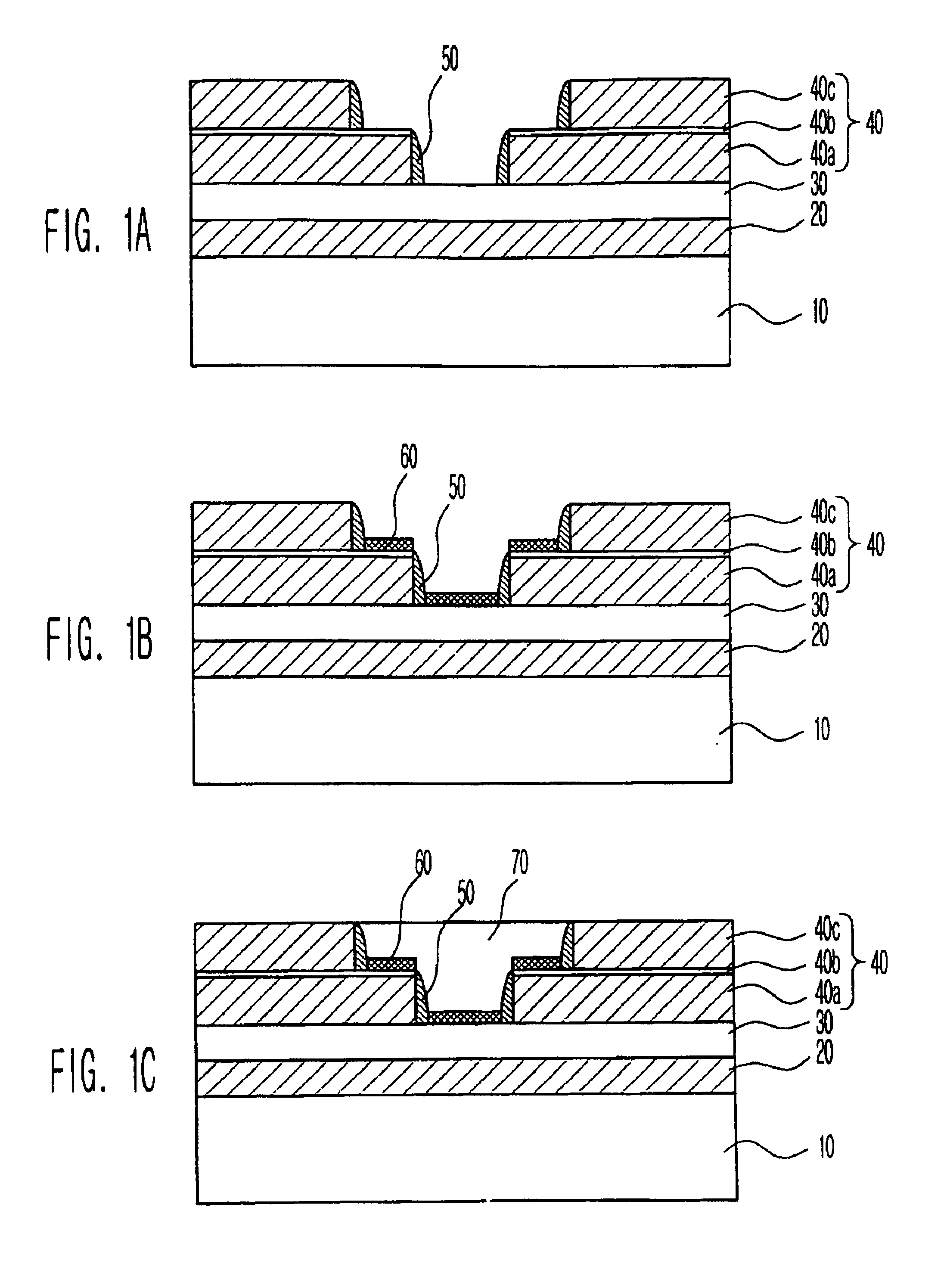
The disclosed method will be described in detail by way of a preferred embodiment with reference to accompanying drawings. Referring now to FIGS. 1A through 1C, a method of forming a metal wiring in a semiconductor device will be below explained in detail.

Referring now to FIG. 1A, a first interlayer insulating film 20, a lower metal layer 30 and a second interlayer insulating film 40 are sequentially formed on a semiconductor substrate 10 in which various components for forming a semiconductor device are also formed. The second interlayer insulating film 40 consists of a first insulating film 40a, a second insulating film 40b and a third insulating film 40c. Of them, the second insulating film 40b comprises a nitride material and serves as an etch prevention film for preventing the first insulating film 40a from being etched upon formation of a trench that is formed during the process of forming a damascene pattern in the second interlayer insulating film 40. Then, a damascene patte...


PUM

PropertyMeasurementUnit
thicknessaaaaaaaaaa
temperatureaaaaaaaaaa
insulatingaaaaaaaaaa

Abstract

A method of forming a metal wiring in a semiconductor device is disclosed. In order to improve a low deposition speed in the process technology by which a damascene pattern of an ultra-fine structure is filled with copper by CVD method, a CECVD method is disclosed by which a chemical enhancer layer for increasing the deposition speed of copper is formed and the damascene pattern is then filled by means of MOCVD method using a copper precursor which forms a copper wiring. A diffusion prevention film is formed on the sidewall of the damascene pattern in the shape of a spacer in order to prevent an increase of the via resistance by the diffusion of copper into the sidewalls of the damascene pattern. A chemical enhancer layer is selectively formed on a lower metal layer that is exposed by the damascene pattern, thus allowing a selective partial filling of the damascene pattern. Therefore, copper filling in an ultra-fine structure is facilitated which also minimizes the electrical resistivity of the copper wiring.

Description

1. Technical FieldA method of forming a metal wiring in a semiconductor device is disclosed. More particularly, the disclosure relates to a method of forming a metal wiring in a semiconductor device by which copper can be selectively filled and an increase of the via resistance in the copper wiring can be prevented with a diffusion prevention film. Still more specifically, a chemical enhancer layer is formed and a damascene pattern of an ultra-fine structure is then filled with copper using a copper precursor.2. Description of the Prior ArtAs the integration level of semiconductor devices is increased and its signal transfer speed is lowered, there has been an effort to use copper as a metal wiring for transferring current because copper has a substantially lower resistivity than conventional aluminum and, conversely, copper has good electrical conductivity.However, copper has a disadvantage that the diffusion speed of copper into a silicon oxide used as an insulating film in a semi...

Claims


Application Information

Patent Timeline
Patent Type & Authority Patents(United States)
IPC IPC(8): H01L21/70H01L21/768H01L21/3205H01L23/52
CPCH01L21/76807H01L21/76831H01L21/76843H01L21/76844H01L21/76876H01L21/76879H01L21/76814H01L21/28
Inventor PYO, SUNG GYU
Owner SK HYNIX INC
Why Eureka
Try Eureka